SPP-IM977
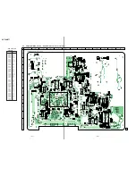
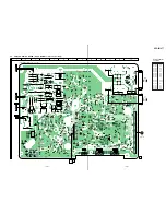
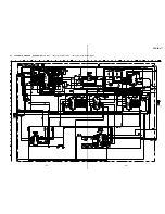
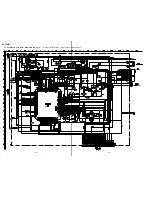
Note on Printed Wiring Board:
•
X
: parts extracted from the component side.
•
Y
: parts extracted from the conductor side.
•
x
: parts mounted on the conductor side.
•
z
: Through hole.
•
b
: Pattern from the side which enables seeing.
(The other layers' patterns are not indicated.)
•
: connected by carbon pattern
– 29 –
– 30 –
4-4.
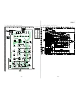
NOTE FOR PRINTED WIRING BOARDS AND SCHEMATIC DIAGRAMS
Caution:
Pattern face side:
Parts on the pattern face side seen from
(Conductor Side)
the pattern face are indicated.
Parts face side:
Parts on the parts face side seen from
(Component Side)
the parts face are indicated.
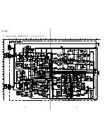
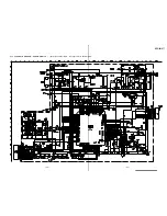
Note on Schematic Diagram:
• All capacitors are in µF unless otherwise noted. pF: µµF
50 WV or less are not indicated except for electrolytics
and tantalums.
• All resistors are in
Ω
and
1
/
4
W or less unless otherwise
specified.
•
%
: indicates tolerance.
•
C
: panel designation.
•
U
: B+ Line.
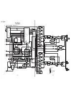
• Power voltages are dc 9 V and fed with regulated dc power
supply from external power voltage jack (J1004) on the
BASE MAIN board, dc 12 V and fed with regulated dc
power supply modular jack (J1003 or J1011) on the BASE
MAIN board with 100
Ω
in series, and dc 3.6 V and fed
with regulated dc power supply battery terminal on the
HAND MAIN board.
• Voltages and waveforms are dc with respect to ground in
test mode.
• Signal path
N
: RX
O
: TX
F
: RX (INTERCOM)
f
: TX (INTERCOM)
P
: BELL
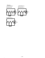
• Waveforms
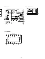
– BASE MAIN Board –
1
U1014
qa
(XOUT)
IV/DIV, 100 ns/DIV
2
U1000
rl
(XTAL1)
400 mV/DIV, 20 ns/DIV
– HAND MAIN Board –
3
U1001
rl
(XTAL1)
400 mV/DIV, 20 ns/DIV
2.8 Vp-p
279 ns
820 mVp-p
54.3 ns
820 mVp-p
54.3 ns
Summary of Contents for SPP-IM977
Page 26: ...SPP IM977 ...
Page 36: ......


