background image

– 20 –

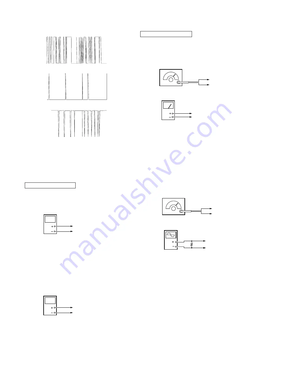
Adjustment Location :  Base main board (see page 21)

 RX Section Adjustment

• Perform the adjustment at T3CH (RX : 46.800MHz) as a rule.

1. IF Adjustment

Setting :

Procedure :

1

FM rf signal generator condition :
Carrier frequency

: 46.800MHz

Modulation

: 1kHz

Deviation

: 3kHz

Output level

: –5dB

µ

V (0.562

µ

V) (EMF)

2

Adjust the T202 for the minimum or the –28dBV reading
on the Level meter.

Adjustment Location :  Hand main board (see page 21)

2. DET Adjustment

Setting :

Procedure :

1

FM rf signal generator condition :
Carrier frequency

: 46.800MHz

Modulation frequency : 1kHz
Deviation

: 3kHz

Output level: 60dB

µ

V (1mV) (EMF)

2

 Adjust the T201 for the maximum reading on the Oscillo-
scope.

Adjustment Location :  Hand main board (see page 21)

FM rf signal

generator

TP76 (ANT)

TP8 (GND)

TP58 (IF)
TP8 (GND)

level meter

FM rf signal

generator

TP76 (ANT)
TP8 (GND)

oscilloscope

TP4 (SP)

TP3 (SP)

200

5-2. HANDSET SECTION

• Apply 4V dc from regulated DC power supply.
• Set to handset manual test mode. (Refer to page 14.)

 TX Section Adjustment

1. TX VCO  Adjustment

• Perform the adjustments at 25CH (49.970MHz) as a rule.

Setting :

Procedure :

1

The digital voltmeter connected TP6 (TX VCO) to TP8
(GND).

2

Adjust the L51 for 1.95 to 2.05V reading on the digital volt-
meter.

Adjustment Location :  Hand main board (see page 21)

2. RX VCO Adjustment

Setting :

Procedure :

1

The digital voltmeter connected TP5 (RX VCO) to TP8
(GND).

2

Adjust the L201 for 2.25 to 2.35V reading on the digital
voltmeter.

Adjustment Location :  Hand main board (see page 21)

digital 

voltmeter

TP6 (TX VCO)

TP8 (GND)

digital 

voltmeter

TP5 (RX VCO)

TP8 (GND)

CH1 DC 500mV/div NORMAL  5mSec/div

CH1

CH1

CH1

DUTY of 50%

DUTY is except 50%

DUTY is except 50%

Summary of Contents for SPP-M100

Page 1: ...ories 2 Handset power source Rechargeable battery pack BP T40 Battery life Standby Approx 30 days Dimensions Approx 23 8 x 81 8 x 23 4 inches w h d antenna excluded Approx 58 x 205 x 69 mm Antenna 31 4 inches 81 mm Mass Approx 10 5 oz Approx 300g battery inclueded Base unit power source DC 9V from AC power adaptor Battery charging time Apprpx 10 hours Dimensions Approx 53 4 x 13 4 x 91 4 inches w ...

Page 2: ...Diagram Base Unit Section 24 6 3 Block Diagram Handset Section 27 6 4 Printed Wiring Boards Base Unit Section 30 6 5 Schematic Diagram Base Unit Section 33 6 6 Schematic Diagram Handset Section 37 6 7 Printed Wiring Boards Handset Section 41 7 EXPLODED VIEWS 7 1 Base Unit Section 47 7 2 Handset Section 48 8 ELECTRICAL PARTS LIST 49 TABLE OF CONTENTS SAFETY RELATED COMPONENT WARNING COMPONENTS IDEN...

Page 3: ... AND FUNCTION OF CONTROLS 1 Hang up tab 2 LINE 2 lamp 3 LINE 1 lamp 4 PAGE button 5 CHARGE lamp 6 Telescopic antenna 7 DIAL MODE switch 8 DC IN 9V jack 9 L2 Telephone jack º L1 or L1 L2 Telephone jack 8 7 6 1 2 3 4 5 9 º BASE UNIT ...

Page 4: ...DIAL PAUSE button 6 PGM button 7 HOLD button 8 CONF button 9 Microphone º FLASH button BATT CHECK button Battery conmpartment SPEED DIAL button RING ON BATT SAVE switch CHANNEL button LINE 2 lamp LINE 1 lamp LINE 2 button ª LINE 1 button º Helical antenna HANDSET º 1 2 3 4 5 6 7 8 9 º ª ...

Page 5: ... 5 This section is extracted from instruction manual ...

Page 6: ... 6 ...

Page 7: ... 7 ...

Page 8: ... 8 ...

Page 9: ... 9 ...

Page 10: ...einthenumericalordergiven r HANDSET 2 1 COVER BATTERY 2 2 REAR CABINET 2 3 HAND MAIN BOARD 2 1 Cover battery 1 Cover bettery 2 Two screws BTP 2 6X12 3 Rear cabinet Two claws Two claws 1 Screw BTP 2 6X8 2 Two screws BTP 2 6X8 4 Hand main board 3 Connector CN502 ...

Page 11: ...his process the machine operates in normal mode How to Release the Test Mode 1 Pull out the AC adapter and turn off the power 2 Remove the short plug and turn on the power again IC501 TP7 TP608 1 22 25 30 35 40 42 5 10 15 20 21 TEST MODE terminal Open Normal Short Test mode How to Release the Test Mode Pull out the AC adapter and turn off the power 1 2 Machine test mode Set the DIAL MODE switch to...

Page 12: ...ng Table During startup in machine test mode make the following chan nel settings by loading the terminal input data Use of under lined channels prohibited in PRISM Pressing the PAGE key in manual test mode switches one by one through the channels starting with channel 1 2 Processing when test mode starts 2 1 Manual test mode If the Test L1 L2 port IC501 ª pin is high for L1 commu nications L1 is ...

Page 13: ...RGE DET DIAL DATA I C 5 0 1 p i n I C 5 0 1 7 p i n H H 8 L L 1 4 Wireless test 4 1 PAGE key processing The channel is incremented only in manual test mode Chan nel incrementing is carried out in 25channel mode Incrementing follows the sequence CH1 n CH2 n nCH24 nCH25 nTInT2 See the channel setting table 4 2 Message transmission reception test 4 2 1 When the ID 3AA Data AAA message is received a m...

Page 14: ...o L if the TEST I O termi nal is at H channel setting and TX ON OFF setting is car ried out Channel setting TX ON OFF setting When the VDET ON terminal is at H the DIP SW condition is input to the key matrix ROW side DIP SW Contents ROW1 P40 IC801 pin Test CH0 Sets the channel number within each group ROW2 P41 IC801 pin Test CH1 Sets the channel number within each group ROW3 P42 IC801 pin Test CH2...

Page 15: ...0 49 080 CH7 H H H L L 44 120 49 100 CH8 L H H L L 44 160 49 160 CH9 H H L H H 44 180 49 200 CH10 L H L H H 44 200 49 240 CH11 H H L H L 44 320 49 280 CH12 L H L H L 44 360 49 360 CH13 H H L L H 44 400 49 400 CH14 L H L L H 44 460 49 460 CH15 H H L L L 44 480 49 500 CH16 L H L L L 46 610 49 670 CH16 H L H H H 46 610 49 670 CH17 H L H H L 46 630 49 845 CH18 L L H H H 46 670 49 860 CH19 L L H H L 46...

Page 16: ...to be no incoming call When it is judged that there is no incoming call the mes sages to the handset are stopped Handset unit When the LINE ring on off message is received from the base the handset blinks the ringing on the handset LINE LED and buzzes the buzzer according to the message Each time the line ring on off message is received from the base the line ring on off check message is transmitt...

Page 17: ... monitored constantly and when it is determined to be high off hook detected Line n is released the base Line n LED goes out and the Line idle shift mes sage is transmitted During Line n hold Line n communication the Line n idle shift message is transmitted during communication and established with back and forth and a half protocol n 1 or 2 Handset unit Reception of the Line idle shift message pu...

Page 18: ...hine test mode Connect to L1 Machine test mode DIAL MODE SW PnTnP TEST I O DIAL MODE SW Press the PAGE key PAGE key OFF L1 L2 PORT L1 L2 PORT Line test L1 L2 PORT 3 party channel test Start manual test mode Normal mode Connect to L2 Set to Test Channel 1 TX ON Redio system test Connect to L1 Connect to L2 Machine test mode L1 L2 PORT Set to Test Channel 0 TX ON L1 DIAL TEST L1 PARA DET L2 RING DET...

Page 19: ... of 50 Since the waveform is not accurately observed adjust so that the top and bottom retrace lines are in the same condi tion FM rf signal generator TP17 ANT TP12 GND TP10 SQ oscilloscope DC range Procedure 1 FM rf signal generator condition Carrier frequency 48 970MHz Modulation frequency 1kHz Deviation 3kHz Output level 60dBµV 1mV EMF 2 Adjust the L4 for the maximum reading on the level meter ...

Page 20: ... generator TP76 ANT TP8 GND TP58 IF TP8 GND level meter FM rf signal generator TP76 ANT TP8 GND oscilloscope TP4 SP TP3 SP 200Ω 5 2 HANDSET SECTION Apply 4V dc from regulated DC power supply Set to handset manual test mode Refer to page 14 TX Section Adjustment 1 TX VCO Adjustment Perform the adjustments at 25CH 49 970MHz as a rule Setting Procedure 1 The digital voltmeter connected TP6 TX VCO to ...

Page 21: ...401 TP402 BASE MAIN BOARD HAND MAIN BOARD TP8 RX VCO Adjustment TP9 TX VCO Adjustment ANT Terminal FM rf signal generator TP401 TP402 TP29 IF Adjustment TP10 SQ SENSITIVITY Adjustment TP5 RX VCO Adjustment TP58 IF Adjustment TP6 TX VCO Adjustment TP76 ANT Terminal FM rf signal generator TP8 GND DET Adjustment TP12 TP17 TP3 TP4 DET Adjustment ...

Page 22: ...lection H L1 L L2 20 10CH 25CH I 10CH 25CH selection H 10CH L 25CH 21 33 40 I Make selection H 33 L 40 22 SQ I Carrier detection H Carrier present 23 BATT LOW I Not used OPEN 24 Not used OPEN 25 BEEP O Beep output terminal 26 DP 1 O Relay RY451 ON OFF control L LINE 1 connected 27 DTMF O DTMF output terminal 28 DP 2 O Relay RY401 ON OFF control L LINE 2 connected 29 Not used OPEN 30 Not used OPEN ...

Page 23: ...N 24 PLL CLK O PLL serial clock output terminal 25 PLL DI O PLL serial data output terminal 26 PLL CE O PLL serial chip enable output terminal 27 30 ROW5 8 O Key output terminal 31 10CH 25CH I 10CH 25CH auto scanning mode select H 10CH L 25CH 32 BATT LOW I Battery low level detection L Battery Low 33 VREG O Regulator output 34 SQ DET I Carrier detection H Carrier present 35 VDET ON O Voltage detec...

Page 24: ...ECTOR CHARGE PUMP UNLOCK DETECTOR FAST LOCK UP A DATA SHIFT REGISTER LATCH 2 LATCH 1 CCB I F PROGRAMMABLE 14bit REFERENCE DIVIDER 16 P18 1 XIN 1 2 24 XOUT 14 PIA 17 VDD 15 VSS 2 CE 3 CL 4 DI 18 CB 5 LDB 23 PDB2 22 PDB1 21 AIB 20 AOB 6 LDA 9 PDA2 10 PDA1 11 AIA 12 AOA 7 CA 13 OUT A 19 OUT B 1 8 CD BIAS CIRCUIT VO2 7 GND 6 VCC 5 VO1 2 FC2 3 FC1 4 VIN 1 2 IC501 9 r WAVEFORMS 2 6Vp p 10 22MHz 6 2Vp p ...

Page 25: ...1 2 3 IC301 r WAVEFORMS 3 9Vp p 4 048MHz 1 3Vp p 10 2MHz 2 2Vp p 32kHz IC801 8 IC801 4 ...

Page 26: ...mark The components identified by mark or dotted line with mark are critical for safety Replace only with part number specified 1 3 570 903 21 LEG B RUBBER 2 3 928 238 01 CABINET LOWER 3 3 928 240 01 LENS 4 3 925 009 11 TERMINAL CHARGE 5 3 928 239 01 BUTTON PAGE 6 3 928 237 01 CABINET UPPER 7 3 925 006 01 HOOK WALL HOOK 8 3 928 241 01 HOLDER LED 9 A 3622 154 A BASE MAIN BOARD COMPLETE 10 3 914 709...

Page 27: ...DER LED 63 A 3672 050 A HAND BOARD COMPLETE 64 3 384 116 01 CUSHION BZ 65 3 918 133 01 CUSHION MICROPHONE 66 3 918 132 01 TERMINAL BATTERY 67 3 914 699 11 TERMINAL CHARGE CHARGE 68 3 915 621 01 HOLDER MICROPHONE 69 X 3369 851 1 CABINET REAR ASSY 70 3 915 612 01 COVER BATTERY 71 3 370 982 01 FOOT H RUBBER 72 1 765 461 11 CORD CONNECTION 73 1 765 612 11 WIRE JUMPER 74 3 930 182 01 LABEL BATTERY CAUT...

Page 28: ...8 1 163 135 00 CERAMIC CHIP 560PF 5 50V C37 1 163 003 11 CERAMIC CHIP 330PF 10 50V C38 1 163 009 11 CERAMIC CHIP 0 001uF 10 50V C101 1 163 245 11 CERAMIC CHIP 56PF 5 50V C102 1 163 121 00 CERAMIC CHIP 150PF 5 50V C103 1 163 037 11 CERAMIC CHIP 0 022uF 10 25V C104 1 163 117 00 CERAMIC CHIP 100PF 5 50V C105 1 163 222 11 CERAMIC CHIP 5PF 0 25PF 50V C107 1 163 033 00 CERAMIC CHIP 0 022uF 50V C108 1 16...

Page 29: ... 50V C460 1 126 963 11 ELECT 4 7uF 20 50V C461 1 136 015 00 CERAMIC CHIP 0 0033uF 50V C501 1 124 910 11 ELECT 47uF 20 50V C503 1 163 031 11 CERAMIC CHIP 0 01uF 50V C504 1 104 666 11 ELECT 220uF 20 10V C505 1 163 031 11 CERAMIC CHIP 0 01uF 50V C506 1 163 237 11 CERAMIC CHIP 27PF 5 50V C507 1 163 237 11 CERAMIC CHIP 27PF 5 50V C551 1 124 910 11 ELECT 47uF 20 50V C602 1 164 222 11 CERAMIC CHIP 0 22uF...

Page 30: ...22 TRANSISTOR 2SA1162 G Q402 8 729 216 22 TRANSISTOR 2SA1162 G Q403 8 729 230 49 TRANSISTOR 2SC2712 YG Q406 8 729 032 66 TRANSISTOR 2SC5069 TD Q451 8 729 216 22 TRANSISTOR 2SA1162 G Q452 8 729 216 22 TRANSISTOR 2SA1162 G Q453 8 729 230 49 TRANSISTOR 2SC2712 YG Q456 8 729 032 66 TRANSISTOR 2SC5069 TD Q602 8 729 807 52 TRANSISTOR 2SD1623 T Q603 8 729 807 52 TRANSISTOR 2SD1623 T Q604 8 729 230 49 TRA...

Page 31: ...GLAZE 100K 5 1 10W R404 1 216 065 00 METAL CHIP 4 7K 5 1 10W R405 1 216 073 00 METAL CHIP 10K 5 1 10W R406 1 216 109 00 METAL CHIP 330K 5 1 10W R407 1 216 089 00 METAL GLAZE 47K 5 1 10W R408 1 216 113 00 METAL CHIP 470K 5 1 10W R409 1 216 065 00 METAL CHIP 4 7K 5 1 10W R410 1 216 089 00 METAL GLAZE 47K 5 1 10W R411 1 216 073 00 METAL CHIP 10K 5 1 10W R412 1 249 393 11 CARBON 10 5 1 4W R451 1 215 8...

Page 32: ...163 033 00 CERAMIC CHIP 0 022uF 50V C220 1 163 129 00 CERAMIC CHIP 330PF 5 50V C221 1 163 235 11 CERAMIC CHIP 22PF 5 50V C222 1 163 235 11 CERAMIC CHIP 22PF 5 50V C223 1 163 038 00 CERAMIC CHIP 0 1uF 25V C224 1 163 009 11 CERAMIC CHIP 0 001uF 10 50V C301 1 163 106 00 CERAMIC CHIP 36PF 5 50V C302 1 163 239 11 CERAMIC CHIP 33PF 5 50V C304 1 164 222 11 CERAMIC CHIP 0 22uF 25V C305 1 162 638 11 CERAMI...

Page 33: ...ZE 0 5 1 10W JR6 1 216 296 00 METAL GLAZE 0 5 1 8W JR7 1 216 295 00 METAL GLAZE 0 5 1 10W JR8 1 216 296 00 METAL GLAZE 0 5 1 8W JR501 1 216 295 00 METAL GLAZE 0 5 1 10W JR502 1 216 296 00 METAL GLAZE 0 5 1 8W JR601 1 216 295 00 METAL GLAZE 0 5 1 10W JR602 1 216 296 00 METAL GLAZE 0 5 1 8W JR923 1 216 295 00 METAL GLAZE 0 5 1 10W JR926 1 216 295 00 METAL GLAZE 0 5 1 10W COIL L51 1 409 673 11 COIL O...

Page 34: ... R535 1 216 085 00 METAL CHIP 33K 5 1 10W R601 1 216 029 00 METAL CHIP 150 5 1 10W R604 1 216 057 00 METAL CHIP 2 2K 5 1 10W R605 1 216 097 00 METAL GLAZE 100K 5 1 10W R606 1 216 057 00 METAL CHIP 2 2K 5 1 10W R607 1 216 097 00 METAL GLAZE 100K 5 1 10W R650 1 216 049 00 METAL GLAZE 1K 5 1 10W R651 1 216 049 00 METAL GLAZE 1K 5 1 10W R652 1 216 049 00 METAL GLAZE 1K 5 1 10W R802 1 216 057 00 METAL ...

Page 35: ...21 ADAPTOR AC AC T47 1 528 764 81 BATTERY LEAD STRAGE 1 775 541 11 CORD WITH MODULAR PLUG LINE FOR LONG 3 800 803 31 MANUAL INSTRUCTION ENGLISH SPANISH CHINESE 3 916 982 01 SHEET ADDRESS 3 931 470 01 CASE WALL HOOK X 3338 101 1 SCREW ASSY TAPESTRY HARDWARE LIST 1 7 685 134 19 SCREW BTP 2 6X8 TYPE2 N S 2 7 685 133 19 SCREW BTP 2 6X6 TYPE2 N S 3 7 685 146 11 SCREW P 3X8 TYPE2 N S 4 7 685 536 11 SCRE...

Reviews: