– 29 –
– 30 –
SPP-N1001/N1003
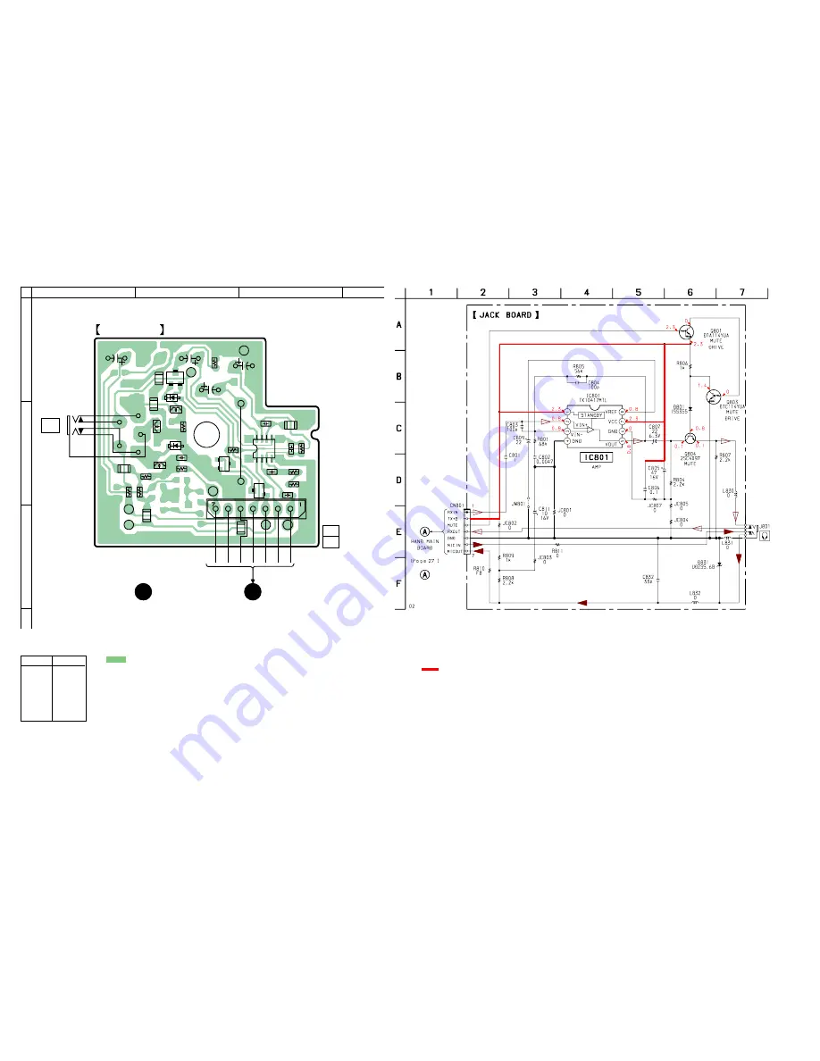
5-8. PRINTED WIRING BOARDS (JACK SECTION) (SPP-N1003 ONLY)
Note:
•
X
: parts extracted from the component side.
•
: Pattern of the rear side.
5-9. SCHEMATIC DIAGRAM (JACK SECTION) (SPP-N1003 ONLY)
D801
A-2
D802
B-2
IC801
B-3
Q801
B-3
Q803
B-2
Q804
A-2
Ref. No.
Location
z
Semiconductor
Location
Note:
• All capacitors are in
µ
F unless otherwise noted. pF:
µµ
F
50 WV or less are not indicated except for electrolytics
and tantalums.
• All resistors are in
Ω
and
1
/
4
W or less unless otherwise
specified.
•
: B+ Line.
• Power voltage is dc 2.4V and fed with regulated dc power
supply from external power voltage jack (J901).
• Voltages are dc with respect to ground in service mode.
• Voltages are taken with a VOM (Input impedance 10 M
Ω
).
Voltage variations may be noted due to normal produc-
tion tolerances.
• Waveforms are taken with a oscilloscope.
Voltage variations may be noted due to normal produc-
tion tolerances.
• Signal path.
N
: RX
O
: TX
02
BCE
ECB
Q801
BCE
YEL
WHT
BLK
BLU
ORG
RED
BWN
A
HAND MAIN BOARD
(FORMER TYPE)(Page 26)
A
HAND MAIN BOARD
(NEW TYPE)
11
(11)
1-678-426-
2
3
A
1
B
C
R805
R806
R807
R808
R809
R810
R811
C801
C803
C806
C832
C804
Q804
D801
Q803
R804
R801
C802
IC801
JC801
JC803
JC804
JC805
JC807
TP807
TP804
TP803
TP801
L832
L830
L831
D831
TP802
TP810
TP809
JC802
CN801
JW801
C807
C811
C809
C805
JACK BOARD
J801
I
1
4
5
8
(FOMER TYPE)
HAND MAIN BOARD
(NEW TYPE)
Summary of Contents for SPP-N1001
Page 3: ... 3 SECTION 1 GENERAL This section is extracted from instruction manual ...
Page 4: ... 4 ...
Page 5: ... 5 SPP N1003 ...
Page 48: ...15 SPP N1001 N1003 ...


