34
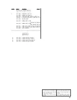
Pin No.
Pin Name
I/O
Function
51
52
53
54
55
56
57
58
59
60
61
62
63
64
65
66
67
68
69
70
71
72
73
74
75
76
77
78
79
80
81
82
83
84
85
86
87
88
89
90
91
92
93
94
95
96
97
98
99
100
CDCICLK
RESETOP
KEYPADC0
KEYPADC1
KEYPADC2
KEYPADC3
KEYPADC4
KEYPADC5
KEYPADC6
KEYPADC7
VSSC
VDDC
TESTP
VSSP
VDDP
GPIOC1/LNAATN
RXEN
GPIOC6/SYNDATA
REFOSC
GPIOC7/SYNCLK
GPIOC5/SYNSTB
GPIOC4/SYNEN
DVDD
DVSS
AVDD
AVSS
BATTERY
VRP
BEEP
TXDATA
RXIP
RXIN
RXQP
RXQN
AGND
RXREF
AGC
RESETIP
TXEN
GPIOC3/TXPWR1
TRSW
GPIOC2/TXPWR0
LCD RS
LCD RW
LCD EN/BATT LOW LED
LCD POWER
DIAL LED
TALK LED/LCD BACK LIGHT
AMP MUTE
VDDC
–
O
–
–
–
–
–
–
–
–
–
–
–
–
–
O
O
O
–
O
O
O
–
–
–
–
I
O
O
O
I
I
I
I
O
–
O
I
O
O
–
O
–
–
O
–
I/O
O
–
–
Bit clock input/output for digital serial interface
Not used (open)
Codec reset
Keypad bidirectional control/LCD data
Keypad bidirectional control/LCD data
Keypad bidirectional control/LCD data
Keypad bidirectional control/LCD data
Keypad bidirectional control/LCD data
Keypad bidirectional control/LCD data
Keypad bidirectional control/LCD data
Not used (open)
VSS supply to core
VDD supply to core
Not used (open)
VSS supply to pad ring
VDD supply to pad ring
LNA select
Receive enable
Synthesizer data
9.6 MHz clock used by synthesizer
Synthesizer clock
Synthesizer strobe
Synthesizer power
VDD supply to A/D converters
VSS supply to A/D converters
VDD supply to analog
VSS supply to analog
Battery voltage input
Analog voltage reference output
AFC DAC output
Transmitter data
Receiver I positive differential input
Receiver I negative differential input
Receiver Q positive differential input
Receiver Q negative differential input
Analog ground
Receiver ADC reference
Not used (open)
AGC control
Power-on reset RC input; active low
Transmit enable
PA power level select
Transmit=1/receive=0 select
Not used (open)
PA power level select
Not used (open)
Not used (open)
BATT LOW LED output
Not used (open)
DIAL LED output
TALK LED output
Not used (open)
VDD supply to core


