– 58 –
•
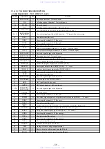
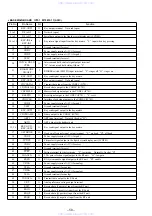
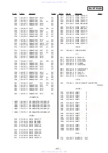
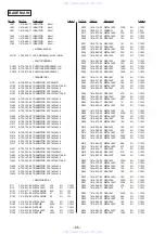
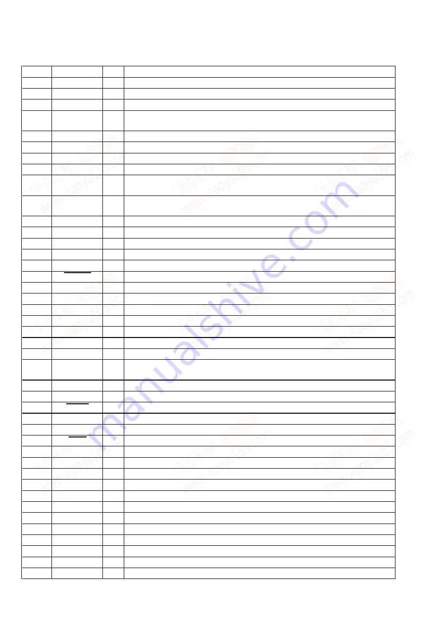
BASE MAIN BOARD IC751 M70012-11 (ASIC)
Pin No.
Pin Name
I/O
Function
1
KEY-OUT5
O
Key output terminal Not used (open)
2 to 5
D0 to D3
O
Not used (open)
6 to 9
D4 to D7
O
Serial data output to the liquid crystal display unit (LCD801)
10 to 15
KEY-IN0 to
KEY-IN5
I
Key return signal input from the key matrix “L” input when key pressing
16
VSSC
—
Ground terminal (for core)
17
VDDC
—
Power supply terminal (+5V) (for core)
18
VDDP
—
Power supply terminal (+5V) (for pad)
19
VSSC
—
Ground terminal (for core)
20
INTC & HOLD
CTRL
O
Intercom and hold control signal output terminal
“H”: intercom and hold status, Others: “L”
21
RING MODE
ON/OFF
I
RINGER switch (SW952) input terminal “L”: ringer off, “H”: ringer on
22
KEY-OUT3
O
Key send signal output to the key matrix
23
KEY-OUT4
O
Key output terminal Not used (open)
24
CDCDATAI
I
Transmit data input from the CODEC (IC701)
25
CDCDATAO
O
Receive data output to the CODEC (IC701)
26
CDCMCLK
O
Master clock signal output to the CODEC (IC701)
27
RESETO
O
Reset signal output to the CODEC (IC701) “L”: reset
28
CDCICLK
O
Interface clock signal output to the CODEC (IC701)
29
VDDP
—
Power supply terminal (+5V) (for pad)
30
VSSP
—
Ground terminal (for pad)
31
KEY-OUT2
O
Key send signal output to the key matrix
32
CDCFRAME
O
Frame output to the CODEC (IC701)
33
ARTI
I
ART input terminal Not used (fixed at “H”)
34
ARTO
O
ART output to the handset unit
35, 36
KEY-OUT1,
KEY-OUT0
O
Key send signal output to the key matrix
37
OFFHOOK
O
Hook on/off control signal output terminal “L”: on hook, “H”: off hook
38
VDDP
—
Power supply terminal (+5V) (for pad)
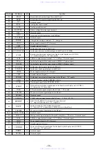
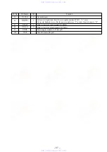
Chip select signal output to the liquid crystal display unit (LCD801)
Power supply terminal (+5V) (for core)
Setting terminal for the test mode “L”: test mode Normally: fixed at “H”
LNA gain selection signal output to the RF unit “H”: low gain
RX system enable signal output to the RF unit “H”: enable
Power supply terminal (+5V) (for analog)
Power supply terminal (+5V) (for analog)
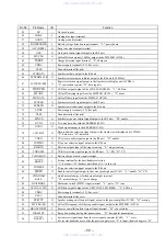
48
VSSA
—
Ground terminal (for analog)
49
TXDATA
O
Transmit data output to the RF unit
50
VRP
O
Analog reference voltage output terminal
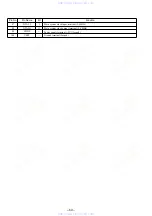
51
RXIP
I
Receive data (I positive) input from the RF unit
52
RXIN
I
Receive data (I negative) input from the RF unit
53
RXQP
I
Receive data (Q positive) input from the RF unit
54
RXQN
I
Receive data (Q negative) input from the RF unit
www. xiaoyu163. com
QQ 376315150
9
9
2
8
9
4
2
9
8
TEL 13942296513
9
9
2
8
9
4
2
9
8
0
5
1
5
1
3
6
7
3
Q
Q
TEL 13942296513 QQ 376315150 892498299
TEL 13942296513 QQ 376315150 892498299

