STR-DA6400ES
153
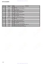
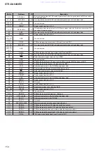
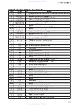
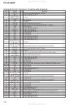
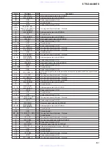
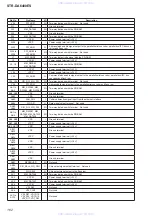
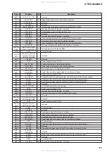
DSP BOARD IC5202 ADSST-AVR-1131 (DSP2)
Pin No.
Pin Name
I/O
Description
A1
CLKCFG0
I
Clock frequency setting terminal
A2
XTAL
O
System clock output terminal (25 MHz)
A3
TMS
I
Mode selection signal input terminal (for JTAG) Not used
A4
TCK
I
Clock signal input terminal (for JTAG) Not used
A5
TDI
I
Data input terminal (for JTAG) Not used
A6
CLKOUT
O
Clock signal output terminal Not used
A7
TDO
O
Data output terminal (for JTAG) Not used
A8
EMU
-
Not used
A9
MOSI
I/O
When DSP2 is master: Serial data output to the serial
fl
ash
When DSP2 is slave: Serial data input from the DSP controller
A10
MISO
I/O
When DSP2 is master: Serial data input from the serial
fl
ash
When DSP2 is slave: Serial data output to the DSP controller
A11
SPIDS
I
Serial data latch pulse signal input from the DSP controller
A12
VDDINT
-
Power supply terminal (+1.2V)
A13, A14
GND
-
Ground terminal
B1
CLKCFG1
I
Clock frequency setting terminal
B2
GND
-
Ground terminal
B3
VDDEXT
-
Power supply terminal (+3.3V)
B4
CLKIN
I
System clock input terminal (25 MHz)
B5
TRST
I
Reset signal input terminal (for JTAG) Not used
B6
AVSS
-
Ground terminal
B7
AVDD
-
Power supply terminal (+1.2V)
B8
VDDEXT
-
Power supply terminal (+3.3V)
B9
SPICLK
I/O
When DSP2 is master: Serial data transfer clock signal input from the DSP controller
When DSP2 is slave: Serial data transfer clock signal output to the serial
fl
ash
B10
RESET
I
Reset signal input from the DSP controller "L": reset
B11
VDDINT
-
Power supply terminal (+1.2V)
B12 to B14
GND
-
Ground terminal
C1, C2
BOOTCFG1,
BOOTCFG0
I
Boot mode setting signal input from the DSP controller
C3, C12,
C13
GND
-
Ground terminal
C14, D1
VDDINT
-
Power supply terminal (+1.2V)
D2,
D4 to D6,
D9 to D11,
D13
GND
-
Ground terminal
-
Power supply terminal (+1.2V)
-
Ground terminal
O
Chip enable signal output to the serial
fl
ash
I
Audio muting control signal input from the digital audio interface receiver or HDMI receiver
O
Interrupt request signal output to the DSP controller
-
Ground terminal
I
PLL lock error signal and data error
fl
ag input from the DSP1
I
Master clock signal input from the digital audio interface receiver or HDMI receiver
G1
AD7
I/O
Two-way data bus with S-RAM and address signal output to the address latch
G2
VDDINT
-
Power supply terminal (+1.2V)
G13
VDDEXT
-
Power supply terminal (+3.3V)
G14
DPBCK
I
Bit clock signal input for PCM audio signal input from the digital audio interface receiver,
DSP1 or HDMI receive
H1
AD6
I/O
Two-way data bus with S-RAM and address signal output to the address latch
H2
VDDEXT
-
Power supply terminal (+3.3V)
H13
DPLRCK
I
L/R sampling clock signal input for PCM audio signal input from the digital audio interface
receiver, DSP1 or HDMI receiver
www. xiaoyu163. com
QQ 376315150
9
9
2
8
9
4
2
9
8
TEL 13942296513
9
9
2
8
9
4
2
9
8
0
5
1
5
1
3
6
7
3
Q
Q
TEL 13942296513 QQ 376315150 892498299
TEL 13942296513 QQ 376315150 892498299


