65
STR-DG910
• IC Pin Descriptions
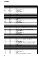
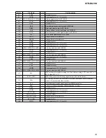
IC1009 ADSP21266SKSTZ-2C (DSP EX3) (DIGITAL BOARD (3/5))
Pin No.
Pin Name
I/O
Pin Description
1
VDDINT
—
Power supply terminal (+1.2 V)
2
CLKCFG0
I
Clock frequency setting signal input 0
3
CLKCFG1
I
Clock frequency setting signal input 1
4
BOOTCFG0
I
Boot mode setting signal input 0 from DSP.
5
BOOTCFG1
I
Boot mode setting signal input 1 from DSP.
6
GND
—
Ground
7
VDDEXT
—
Power supply terminal (+3.3 V)
8
GND
—
Ground
9
VDDINT
—
Power supply terminal (+1.2 V)
10
GND
—
Ground
11
VDDINT
—
Power supply terminal (+1.2 V)
12
GND
—
Ground
13
VDDINT
—
Power supply terminal (+1.2 V)
14
GND
—
Ground
15
INT_REQ
O
Interrupt status output for main system controller.
16
DIR_ERR
O
PLL lock error signal and data error flag output for main system controller.
17
AD7
I/O
Two-way data bus and address signal output 7 with S-RAM. (Not used in this set)
18
GND
—
Ground
19
VDDINT
—
Power supply terminal (+1.2 V)
20
GND
—
Ground
21
VDDEXT
—
Power supply terminal (+3.3 V)
22
GND
—
Ground
23
VDDINT
—
Power supply terminal (+1.2 V)
24 to 26
AD6 to AD4
I/O
Two-way data bus and address signal output 6 to 4 with S-RAM. (Not used in this set)
27
VDDINT
—
Power supply terminal (+1.2 V)
28
GND
—
Ground
29, 30
AD3, AD2
I/O
Two-way data bus and address signal output 3, 2 with S-RAM. (Not used in this set)
31
VDDEXT
—
Power supply terminal (+3.3 V)
32
GND
—
Ground
33, 34
AD1, AD0
I/O
Two-way data bus and address signal output 1, 0 with S-RAM. (Not used in this set)
35
XWR
O
Data write enable signal output for S-RAM. (L: active) (Not used in this set)
36, 37
VDDINT
—
Power supply terminal (+1.2 V)
38
GND
—
Ground
39
XRD
O
Read strobe signal output for S-RAM. (L: active) (Not used in this set)
40
ALE
O
Address latch enable signal output (Not used in this set)
41 to 43
AD15 to AD13
I/O
Two-way data bus and address signal output 15 to 13 with S-RAM.
(Not used in this set)
44
GND
—
Ground
45
VDDEXT
—
Power supply terminal (+3.3 V)
46
AD12
I/O
Two-way data bus and address signal output 12 with S-RAM. (Not used in this set)
47
VDDINT
—
Power supply terminal (+1.2 V)
48
GND
—
Ground
49 to 52
AD11 to AD8
I/O
Two-way data bus and address signal output 11 to 8 with S-RAM.
(Not used in this set)
53
A16
O
Address signal output 16 for S-RAM. (Not used in this set)
54
VDDINT
—
Power supply terminal (+1.2 V)
55
GND
—
Ground
56, 57
A17, A18
O
Address signal output 17, 18 for S-RAM. (Not used in this set)
58
GND
—
Ground
59
VDDEXT
—
Power supply terminal (+3.3 V)
60
VDDINT
—
Power supply terminal (+1.2 V)
Summary of Contents for STR-DG910
Page 105: ...105 STR DG910 MEMO ...


