background image

STR-DN1070

85

Pin No.

Pin Name

I/O

Description

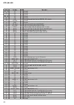
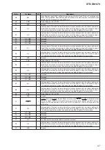
A1, A2

GPIO14, GPIO12

-

Not used

A3

SDA

I/O

Two-way I2C data bus terminal    Not used

A4

USB_DP_P1

I/O

Two-way USB serial data (+) bus terminal

A5

USB_DP_P0

-

Not used

A6

USB_VRT_P0P1

-

External reference resistor connection terminal

A8

NC

-

Not used

A9

NC

-

Not used

A11

NC

-

Not used

A12

NC

-

Not used

A14

NC

-

Not used

A15

NC

-

Not used

A16

NC

-

Not used

A17

NC

-

Not used

A19

NC

-

Not used

A20

NC

-

Not used

A22

RSTI

-

Not used

A24

AOMCLK

O

Master clock signal output to the stream processor

A25

AOBCK

O

Bit clock signal output to the stream processor and RF modulator

A26

AOSDATA2

O

Digital audio signal output to the stream processor

A27

AOSDATA4

O

Digital audio signal output terminal

A28

AR0

-

Not used

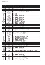
B1

GPIO25

-

PCM and DSD selection for multiplexer

B2

GPIO24

-

MTK_XPCM_DSD_SEL_IN

B3

SCL

I/O

Two-way I2C clock bus terminal    Not used

B4

USB_DM_P1

I/O

Two-way USB serial data (-) bus terminal

B5

USB_DM_P0

-

Not used

B8

NC

-

Not used

B9

NC

-

Not used

B11

NC

-

Not used

B12

NC

-

Not used

B14

NC

-

Not used

B15

NC

-

Not used

B16

NC

-

Not used

B17

NC

-

Not used

B19

NC

-

Not used

B20

NC

-

Not used

B22

NC

-

Not used

B23

OPTICAL

I

Digital audio signal input from the optical/coaxial receiver

B24

AOSDATA0

O

Digital audio signal output to the stream processor

B25

AOSDATA1

O

Digital audio signal output to the RF modulator

B26

AOSDATA3

O

Not used

B27

AOLRCK

O

L/R sampling clock signal output to the stream processor and RF modulator

B28

AL0

-

Not used

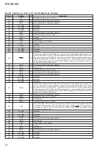
C1

GPIO15

O

Request signal output to the system controller

C2 to C5

GPIO26, GPIO13,

GPIO10, GPIO11

-

Not  used

C7

NC

-

Not used

C9

NC

-

Not used

C10

NC

-

Not used

C11

NC

-

Not used

C12

NC

-

Not used

C13

NC

-

Not used

C14

NC

-

Not used

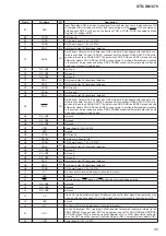
C15

AVDD12_2

-

Power supply terminal (+1.2V)

•  IC Pin Function Descriptions
MB-1512 BOARD (1/16), (2/16), (4/16), (5/16), (6/16) IC101 CXD90028GB-B-E (BD DECODER)

Summary of Contents for STR-DN1070

Page 1: ... Inc This product incorporates Spotify software which is subject to 3rd party licenses found here https developer spotify com esdk third party licenses Spotify and Spotify logos are trademarks of the Spotify Group This function may not be available in some countries regions All other trademarks and registered trademarks are of their respective holders In this manual and marks are not specified Not...

Page 2: ...enna s performance operating system software application etc 2 BLUETOOTH standard profiles indicate the purpose of BLUETOOTH communication between devices 3 Codec Audio signal compression and conversion format 4 Subband Codec General Power requirements Area Power requirements US Canadian 120 V AC 60 Hz AUS 230 V AC 50 Hz AEP UK 230 V AC 50 60 Hz Power consumption 240 W Power consumption during sta...

Page 3: ... this job 3 Measuring the voltage drop across a resistor by means of a VOM or battery operated AC voltmeter The limit indication is 0 75 V so analog meters must have an accurate low voltage scale The Simpson 250 and Sanwa SH 63Trd are examples of a passive VOM that is suitable Nearly all battery operated digital multimeters that have a 2 V AC range are suitable See Fig A 1 5 kΩ 0 15 μF AC voltmete...

Page 4: ...Diagram MB 1512 Board Suffix 11 21 10 16 50 6 22 Schematic Diagram MB 1512 Board Suffix 11 21 11 16 51 6 23 Schematic Diagram MB 1512 Board Suffix 11 21 12 16 52 6 24 Schematic Diagram MB 1512 Board Suffix 11 21 13 16 53 TABLE OF CONTENTS 6 25 Schematic Diagram MB 1512 Board Suffix 11 21 14 16 54 6 26 Schematic Diagram MB 1512 Board Suffix 11 21 15 16 55 6 27 Schematic Diagram MB 1512 Board Suffix...

Page 5: ...are damaged ex change the entire mounted board MODEL IDENTIFICATION BACK PANEL Model Part No US Canadian 4 581 825 0 AEP UK 4 581 825 1 Australian 4 581 825 2 NOTE OF REPLACING THE WLAN BT COMBO CARD When the WLAN BT COMBO CARD is exchanged the MAC address has been changed Please print and cut out the following explanations and return it with the unit that complete the repair MAC address of this r...

Page 6: ... of IC1911 IC1912 IC1913 and IC1916 on the DCDC Board used in this unit required to unsolder the grounding wire on the DCDC Board Grounding wire After replaced the IC1911 IC1912 IC1913 and IC1916 have to solder back the grounding wire on the DCDC Board properly before turn on the set refer image provided below Caution If insufficient solder occured for the grounding wire in DCDC Board it may cause...

Page 7: ...ional speaker until you detect which speaker is causing the protection error After checking the above items and fixing any problems plug in the AC power cord mains lead and turn on the receiver If the problem persists consult your nearest Sony dealer An over current from the USB port was detected Disconnect the USB devices as prompted in the warning message and close the message For other messages...

Page 8: ...the m button on the remote commander to select 6 P2P Registry Check Screen 6 13 Press the button on the remote commander to check the P2P device address is the same as shown in Screen 5 Displayed characters values in the following figure are example 14 Press the BACK button on the remote commander and select Factory Initialize go to Screen 7 15 The set will turn off automatically Diag Category Blu...

Page 9: ...he numerical order given 2 2 CASE STEPUP 3 four screws BVTP 3 u 8 4 1 three screws B TYPE 4 u 8 2 three screws B TYPE 4 u 8 5 case stepup 4 2 2 CASE STEPUP Page 9 2 6 BACK PANEL SECTION Page 13 2 7 STANDBY BOARD MAIN BOARD SECTION Page 14 2 8 MAIN BOARD Page 14 2 5 MB 1512 BOARD Page 12 2 4 FRONT PANEL SECTION Page 11 2 3 WLAN BT COMBO CARD Page 10 SET ...

Page 10: ...s removed from the clamp L35 2 connector 8P 4 cushion R cushion R cushion R 6 cushion R 3 wireless LAN antenna connector 1 5 wireless LAN antenna connector 2 7 wireless LAN antenna connector 3 card WLAN BT combo rear side LUH VHWWLQJ rear side clamp L35 card WLAN BT combo DCDC board LUH VHWWLQJ Note When the WLAN BT combo card is replaced refer to NOTE OF REPLACING MB 1512 BOARD OR WLAN BT COMBO C...

Page 11: ...3 u 8 1 Cut the cable tie 4 Cut the cable tie 6 CN501 5P 7 CN1391 4P rear side front side pin lead shield sub chassis N104 T901 cable tie cable tie clamp L35 pin lead heat sink SQ N86 SUPPORT board LUH VHWWLQJ LUH VHWWLQJ LUH VHWWLQJ 2 HDMI cable 420mm CN3500 3 wire flat type 27 core CN3004 5 Wire is removed from the clamp L35 ...

Page 12: ...ws BVTP 3 u 8 8 one screw BVTP 3 u 8 1 wire flat type 22 core CN8002 L E E F G H I F H I G L 2 CN8000 13P 3 CN8004 2P 4 CN8003 12P 5 wire flat type 22 core CN8001 6 CN301 10P 0 one screw BVTP 3 u 8 EXCEPT US CND one screw BV 3 u 8 CU US CND qa seven screws B 3 u 5 LUH VHWWLQJ rear side clamp L35 clamp L35 DCDC board LUH VHWWLQJ qh tape qh tape qg rivet DIA 3 nylon 37 86 1 K K J J 2 5 MB 1512 BOARD...

Page 13: ...1907 2P 5 CNP901 3P 4 CN1905 4P 7 six screws BVTP 3 u 8 8 seven screws BVTP 3 u 8 9 back panel section 6 five screws BVTP 3 u 8 US CND five screws BV RING EXCEPT US CND LUH VHWWLQJ clamp L35 DCDC board 1 Wire is removed from the clamp L35 3 Wire is removed from the clamp L35 ...

Page 14: ... 4 INSULATION board 2 SUPPORT board 5 one screw BVTP 3 u 8 7 one screw BVTP 3 u 8 7 one screw BVTP 3 u 8 8 bracket support beam 8 bracket support beam 6 USB INSULATION board LUH VHWWLQJ LUH VHWWLQJ pin lead cable tie cable tie T901 MAIN board 9 one screw BVTP 3 u 8 3 four screws BVTP 3 u 8 4 STANDBY board 2 CNP902 4P 6 CNP920 5P 7 CNP930 5P 8 two screws BVTP 3 u 8 8 two screws BVTP 3 u 8 rear side...

Page 15: ...and PURE DIRECT buttons simultaneously press the 1 button to turn on the main power 2 The message REST XX appears Every pressing of any button other than the 1 counts down the buttons 3 The buttons which are already counted once are not counted again 4 When all buttons are pressed REST 00 appears SWAP ALL MODE The signal will be swap to all channels so that all speakers will have sound output Proc...

Page 16: ...r the message below appears Select the desired mode Items Display AV1 C M O D E A V 1 AV2 C M O D E A V 2 SPECIAL MODE Enable user or service or factory or designer to access test mode Procedure 1 Press the 1 button to turn the power on 2 While pressing DISPLAY MODE button press and release the 2CH MULTI MOVIE MUSIC button in order 3 The message SPECIALIZE appear 4 To enter SPECIAL Menu List press...

Page 17: ... pressing DISPLAY MODE button press and release the MUSIC MOVIE 2CH MULTI button in order 3 The message REMOTE OFF appears and switch on the set SVC SERVICE MODE Note The operation in this mode must use a remote commander and TV monitor Setting method of the SVC service mode 1 Connect this unit with TV monitor 2 Press the 1 button to turn the power on 3 While pressing DISPLAY MODE button press and...

Page 18: ...io Input Test Not used LUHOHVV 1 7HVW 3 3 WHVW RQO 0 7HVW 0RGH Not used Drive Not used 5 7HVW 0RGH Not used Start Initialize QLWLDOL H GHIDXOW VHWWLQJ IRU WKH XQLW LDJ 7HVW Transcoder Test Not used 0 QSXW 7HVW Not used OXHWRRWK HYLFH 7HVW 0LF 7HVW Not used 0RGH Not used Not used Service 0ode 0enu 1 DiaJ LoJ 3 Factory Initialize 4 Network 5 Version Up 6 System Information Service 0ode 0enu 1 DiaJ L...

Page 19: ...t This screen is used to test devices mounted on the board Screen 1 Selects the test category Operation Selects the category m Moves to the selected category BACK Returns to the service top menu Screen 2 Device test Selects the device to test after selecting Device Test in screen 1 Operation Selects the device to test Executes the test M Returns to selection of test category BACK Returns to select...

Page 20: ...oint 3 Start Display RSSI Value 4 Start Ping Test 5 Write P2P address to Registry 6 P2P Registry Check P2P device address xx xx xx xx xx xx HELP UP DOWN ENT RET Screen 1 Screen 2 Screen 3 8 Diag MIC Input Test This screen performs MIC input test Note Not used for the servicing 9 Diag HDMI Input Test This screen performs HDMI input test Note Not used for the servicing 10 Diag Transcoder Test Note N...

Page 21: ...age BACK Returns to the screen Screen 1 that selects the log type RED Writes the log contents to an USB memory device Viewing the log display Error Log 174 2010 01 01 00 00 08 ErrCode 0902A4053002 Index number Date Time Error code About copying log to USB memory device Press the RED button in each log display screen with the USB memory device inserted into the unit Note Please do not press the RED...

Page 22: ...n displayed go to Screen 2 BACK Returns to service top menu Screen 2 Basic Information continue Operation Basic Information displayed go to Screen 1 BACK Returns to service top menu When delta IOP is measured it becomes impossible to use the Version Up function Contents List Main LSIname Model Destination Sequence Number MAC IP IF con Main Version IFCon ADSP Coeff Version Bootloader Version Host M...

Page 23: ...kHz Modulation 1 kHz ANT input 35 dBu EMF Note Use 75 ohm coaxial cable to connect signal generator and the set You cannot use video cable for checking Use signal generator whose output impedance is 75 ohm 3 Set to FM tuner function and scan the input FM signal with automatic scanning 4 Confirm that input frequency of A B and C are detected and automatic scanning stops When the station signal is r...

Page 24: ...r transistor example Q1600 on the MAIN board the power amplifier and the surrounding circuit are not defect Check that the surrounding circuit of current detect example Q1600 and Q1601 on the MAIN board is not defect Check the surrounding circuit of protector example Q1604 on the MAIN board and exchange the defective parts Check that between the 59 V line 59 V B line and the ground does not short ...

Page 25: ...board IC6002 pin 16 19 20 21 Check the following parts and the surrounding circuit and exchange the defective parts MB 1512 board IC3002 IC6500 IC6501 Check the following parts and the surrounding circuit and exchange the defective parts MB 1512 board IC3002 IC6000 Check the following parts and the surrounding circuit and exchange the defective parts MB 1512 board IC3002 MAIN board IC1414 Perform ...

Page 26: ...cuit and exchange the defective parts MAIN board IC1231 MB 1512 board IC6002 Check the following parts and the surrounding circuit and exchange the defective parts MB 1512 board IC6000 Check that OPT is displayed on the fluorescent indicator Check the following parts and the surrounding circuit and exchange the defective parts MAIN board IC1414 J1401 J1402 Check that the sound from the optical inp...

Page 27: ...11 IC1912 IC1913 IC1916 F940 Check the following parts and the surrounding circuit and exchange the defective parts MB 1512 board IC5004 Check the following parts and the surrounding circuit and exchange the defective parts MB 1512 board IC3001 IC3002 Check the following parts and the surrounding circuit and exchange the defective parts MB 1512 board X3000 Check that voltage of the following pin i...

Page 28: ...k that the speaker pattern setting is normal Explain the settings of this unit to the customer Check the surrounding circuit of power transistor of the channel to which data is not outputted example Q1600 on the MAIN board and the surrounding circuit of power amplifier circuit example FL FR on the MAIN board and exchange the defective parts OK NG NG ...

Page 29: ...h R ch R ch R ch FL CIN 2 OUT2 SWIN 1 OUT1 LINE AMP IC1413 51 6 2 1 52 7 R ch SW C SYSTEM CONTROLLER IC3002 1 5 142 TUNER_MOSI 16 X1 17 X2 143 TUNER_CLK EVOL_DATA DA CL EVOL_CLK 55 56 ZONE2_PREOUT_SW_RY 81 42 43 1 2 44 45 57 9 8 11 10 SUBR 25 SBL 12 R ch R ch C R ch 13 OUTSBL OUTSBR 15 R ch 14 31 32 38 39 36 37 56 AUDIO AMP IC1101 R ch R ch R ch R ch R ch R ch R ch INL6 INR6 34 35 R ch R ch R ch 7...

Page 30: ... SWSEL_A1 SWSEL_B1 SW_ 5V2 23 ADINL ADINR VOUT7 VOUT8 29 24 SBL BINARY COUNTER IC6004 MUTE SELECTOR IC6005 SD RAM IC6500 D6003 D8001 FS_RATE 1CK 2QD 88 6LJQDO SDWK AUDIO AUDIO DIGITAL 5 FK LV RPLWWHG GXH WR VDPH DV FK 5 2 3 6 MCKOUT 13 MCLK_IN 92 LRCKOUT 15 LRCLK_IN 97 BCKOUT 14 BCLK_IN 75 MUTEB MCKOUT 13 XMCK 30 24 B Y SELECT VOUT 2 5 A 1 6 SIGNAL SELECTOR IC6012 2 5 6 SIGNAL SELECTOR IC6013 MPIN...

Page 31: ... Q1855 SL LIMITER Q1552 Q1553 BOOSTER Q1550 CURRENT DETECT Q1554 CURRENT DETECT Q1555 BOOSTER Q1551 LIMITER Q1602 Q1603 BOOSTER Q1600 CURRENT DETECT Q1604 CURRENT DETECT Q1605 BOOSTER Q1601 SYSTEM CONTROLLER IC3002 3 5 C PROTECT TEMP_SENSOR1 TEMP_SENSOR3 LIMITTER HP_RY FRONT_SPK_RY SBL_SBR_RY C_RY HP_DET LIMITER Q1802 Q1803 BOOSTER Q1800 CURRENT DETECT Q1804 CURRENT DETECT Q1805 PROTECTOR Q1320 Q1...

Page 32: ... RCS_ AE9 AF13 L3 L2 WE RBA0 AC10 M2 BA0 RBA1 AC15 N8 BA1 RBA2 AG10 M3 BA2 CS RCAS_ RRAS_ AD10 AE11 K3 J3 CAS RAS RCKE AH13 K9 CKE RCLK0 AG17 J7 CK RCLK0_ AH17 K7 CK RDQM1 RDQS1 AE17 AH18 D3 C7 DMU DQSU RDQS1_ RDQM0 AG18 AH19 B7 E7 DQSU DML RODT AE10 K1 ODT RDQS0 AG16 F3 DQSL RDQS0_ AH16 G3 DQSL T2 RESET A0 A12 NC NC DQL0 DQL7 DQU0 DQU7 SD RAM IC103 RDQ16 RDQ31 RCLK1 AG6 RCLK1_ AH6 RDQM3 RDQS3 AH4...

Page 33: ...TA0 DATA0 CLOCK CLOCK SCL 5V SDA 5V HOT PLUG DET CEC 5V POWER 103 102 100 99 96 95 94 93 108 107 RX1P5V 72 8 P1TX2P 3 2 6 7 P1TX2M P1TX1P P1TX1M P1TX0P P1TX0M P1TXCP P1TXCM P0TX2P P0TX2M P0TX1P P0TX1M P0TX0P P0TX0M P0TXCP P0TXCM HSDA0 HSCL0 SYSCLK XI 10 11 13 14 16 17 19 22 24 25 27 28 30 31 33 80 79 77 76 74 73 71 70 7 3 008B DIGITAL VIDEO SECTION 2 2 Page 34 010B DIGITAL VIDEO SECTION 2 2 Page 3...

Page 34: ... DATA1 DATA1 DATA0 DATA0 CLOCK CLOCK 6 9 6 9 HOT PLUG DET CEC 5V POWER 1 B6 6 B 9 6 6 B 6 6 B 1 B6 1 B6 1 B6 IN6_UCOM_HPD 3 6 7 Q5001 D2 _2 D2 _2 D1 _2 D1 _2 D0 _2 D0 _2 CLK _2 CLK _2 6 6 HPD2 P1RX2P P1RX2M P1RX1P P1RX1M P1RX0P P1RX0M P1RXCP P1RXCM 5 6 5 6 P0RX2P P0RX2M P0RX1P P0RX1M P0RX0M P0RX0P P0RXCP P0RXCM 5 6 5 6 6 DO IO1 DI IO0 CLK CH2_P CH2_M CH1_P CH1_M CH0_P CH0_M CLK_P CLK_M 0 6 0 6 HTP...

Page 35: ...RY 62 PURE_DIRECT_LED 124 FLASH_CLK PWR_LED 61 STANDBY_LED 75 AC CUT 79 BRIDGEABLE_RY 42 40 38 51 FL_LAT 60 FL_CLK 59 FL_DATA 93 VOLUME_JOG 90 INPUT_JOG 58 POWER_KEY 91 AD_KEY1 92 AD_KEY2 86 X0 CLOCK IN NFC MODULE 87 X1 SWITCHING TRANSISTOR Q3190 RELAY DRIVER Q951 Q953 1 VIN1 16 14 VIN2 SW2 3 SW1 1 FRONT USB VBUS IC503 5 8 EN VCC 5V REG IC3191 4 52V REG IC1916 5 2V REG IC319 1 8 VO VCC 5V REG IC12...

Page 36: ...tion of transistor C B These are omitted E Q Abbreviation AUS Australian model CND Canadian model Replacement of Q1550 Q1551 Q1600 Q1601 Q1650 Q1651 Q1700 Q1701 Q1750 Q1751 Q1800 Q1801 Q1850 and Q1851 on the MAIN board used in this unit requires L type screw driver Replacement of Q1550 Q1551 Q1600 Q1601 Q1650 Q1651 Q1700 Q1701 Q1750 Q1751 Q1800 Q1801 Q1850 and Q1851 on the MAIN board used in this ...

Page 37: ... R5089 C6051 R3532 C6052 R3533 C6053 C6054 R329 1 5 6 7 CN501 C6055 C6056 1 8 9 10 CN503 R6030 R5090 R6031 R5091 R5092 R6033 R5093 R6048 R5094 R330 R331 R332 R6037 R5097 R333 R6038 R5098 R334 R6039 R5099 R335 R336 C6062 R337 R338 R339 C6066 C6067 R6040 R3548 C3570 R6041 R3549 R6042 R6043 R6044 R340 R6045 R341 R6046 R536 R342 R6047 R343 R6053 R3550 C3190 R6049 C3191 C3192 R3553 C3193 R3554 Q3190 E ...

Page 38: ... FB6501 C3549 R3522 JL2002 JL2003 R318 1 5 6 JL2004 R319 JL2005 JL2006 JL2007 2 1 3 IC6017 R5080 R3528 JL2008 2 1 3 IC6018 C3550 R3529 JL2142 C3553 R320 R3530 R518 JL2010 C3558 R3531 R325 JL2011 1 2 3 IC6021 C3559 R326 JL2012 R327 JL2013 R3534 R328 JL2014 R3535 JL2015 R3536 JL2016 R3537 JL2017 R3538 JL2018 C3560 R3539 C3561 R6032 C3562 C3563 C3564 R6035 R5095 C3565 C101 R6036 R5096 C3566 C102 C356...

Page 39: ... R5093 R6048 R5094 R330 R331 R332 R6037 R5097 R333 R6038 R5098 R334 R6039 R5099 R335 R336 C6062 R337 R338 R339 C6066 C6067 R6040 R3548 C3570 R6041 R3549 R6042 R6043 R6044 R340 R6045 R341 R6046 R536 R342 R6047 R343 R6053 R3550 C3190 R6049 C3191 C3192 R3553 C3193 R3554 Q3190 E K A C3194 R3555 Q3191 C6075 C3195 Q3192 C6076 C3196 C6077 C3197 C2003 R6050 C3199 R6052 R6034 C314 R6055 C315 R6056 R352 C31...

Page 40: ...529 JL2142 C3553 R320 R3530 R518 JL2010 C3558 R3531 R325 JL2011 1 2 3 IC6021 C3559 R326 JL2012 R327 JL2013 R3534 R328 JL2014 R3535 JL2015 R3536 JL2016 R3537 JL2017 R3538 JL2018 C3560 R3539 C3561 R6032 C3562 C3563 C3564 R6035 R5095 C3565 C101 R6036 R5096 C3566 C102 C3567 C103 R3540 C3568 C104 R3541 R3542 C106 R3543 C6063 R3544 C6064 R3545 C6065 R3546 R3547 R530 R531 C3571 R532 C3572 R533 C3573 R534...

Page 41: ...u C140 0 1u C101 0 1u C180 0 1u C181 0 1u C182 0 1u C137 10u C156 10u C175 4p C178 100p C177 4p C176 100p C179 0 1u C121 0 01u C118 0 1u C115 0 1u C106 0 1u CL107 CL108 CL109 CL112 CL113 CL114 CL115 CL116 CL117 CL118 CL120 CL121 CL2118 CL123 CL124 CL125 CL126 CL127 CL128 CL129 CL130 CL131 CL132 CL133 CL134 CL135 CL2101 CL2102 CL2103 CL2104 CL2105 CL2106 CL2117 CL2116 CL122 CL2115 CL2114 CL2113 CL2...

Page 42: ...WE 19 WP 20 NC_20 21 NC_21 22 NC_22 23 NC_23 24 NC_24 25 NC_25 26 NC_26 27 NC_27 28 NC_28 29 I O1 30 I O2 31 I O3 32 I O4 33 NC_33 34 NC_34 35 NC_35 36 VSS_36 37 VCC_37 38 NC_38 39 NC_39 40 NC_40 41 I O5 42 I O6 43 I O7 44 I O8 45 NC_45 46 NC_46 47 NC_47 48 NC_48 GND GND NAND FLASH IC2001 FLASH IC101 2 15 CXD90028GB B E BD DECODER IC101 IC101 5 15 CXD90028GB B E BD DECODER IC101 IC101 6 15 CXD9002...

Page 43: ...15 USB_5 2V JL312 JL313 0 0022u C317 0 1u C318 0 0022u C319 3 3V REG IC318 1V REG IC314 3 3V REG IC324 JL307 JL308 2 2k R388 5 6k R387 10u C335 10u C334 0 01u C336 1k R355 RP108J081D FE IC315 CE 1 VDD 2 GND 3 VOUT 4 VFB 5 6 6 1 8V REG IC315 470u 4V C384 2 2k R319 680 R385 3 3k R320 10u C312 10u C311 0 01u C313 1k R318 RP108J081D FE IC305 CE 1 VDD 2 GND 3 VOUT 4 VFB 5 6 6 1 2V REG IC305 MTK_1 2V JL...

Page 44: ...NT USB_PCONT STRAP_GPIO9 OCPI XIF_CS WIFI_PCONT MTK_MUTE 100 R479 WLAN_SYNC 100 R481 STREAM_STATUS MTK_XPCM_DSD_SEL_IN IF_SCK IF_SDI START_BIT STRAP_GPIO9 XIF_CS OCPI SYS_REQ MTK_MUTE USB_PCONT IF_SDI IF_SCK CLK UPG_STATUS WOL_INT OPWRSB WIFI_PCONT IF_SDO STRAP_XAMUTE START_BIT STRAP_GPIO9 XIF_CS OCPI WLAN_SYNC WLAN_SYNC SYS_REQ MTK_MUTE STREAM_STATUS STREAM_STATUS USB_PCONT IF_SDI IF_SCK UPG_STAT...

Page 45: ... ET501 MTK_3 3V USB_5 2V USB_RF_3 3V MTK_3 3V MTKSTB_3 3V MTKSTB_3 3V J503 8P 1 2 3 4 5 6 7 8 JL503 JL504 JL507 JL506 0uH L502 0uH L501 10k R532 10k R533 75 RB501 10k R534 10k R535 0 R507 10k R531 0 R508 0 R515 WLAN BT COMBO CARD 1k R530 24k R518 5 1k R505 5 1k R504 0 R514 USB_PCONT OCPI WLAN_SYNC IN 1 GND 2 EN 3 FAULT 4 ILIM 5 OUT 6 T501 T502 GND GND GND ET503 GND DM VBUS DP DP DM GND DM DM2 DP2 ...

Page 46: ...K R12 DGND12_K T12 DGND12_K U12 DGND12_K V12 DGND12_K AB12 DGND12_K J13 DGND12_K K13 DGND12_K L13 DGND12_K M13 DGND12_K N13 DGND12_K P13 DGND12_K R13 DGND12_K T13 DGND12_K U13 DGND12_K V13 DGND12_K L14 DGND12_K M14 DGND12_K N14 DGND12_K P14 DGND12_K R14 DGND12_K G14 DVCC33_IO_1 H14 DVCC33_IO_1 G8 DVCC33_IO_2 H8 DVCC33_IO_2 U21 DVCC33_IO_4 V21 DVCC33_IO_4 G22 DVCC33_IO_5 F23 DVCC33_IO_5 AE19 DVCC33...

Page 47: ... 0uH FB5006 0uH JL5007 JL5002 JL5003 JL5004 JL5008 JL5005 JL5006 1 TX0SDA 2 TX0HPD 3 D0 4 D1 5 D2 6 D3 7 D4 8 D5 9 VSS_9 10 D6 11 VDD11_11 12 D7 13 D8 14 D9 15 D10 16 D11 17 VSS_17 18 VDD11_18 19 P1TX2P 20 AVDD11TX_20 21 P1TX2M 22 P1TX1P 23 AVDD11TX_23 24 P1TX1M 25 P1TX0P 26 AVDD33TX_26 27 P1TX0M 28 P1TXCP 29 AVDD11TX_29 30 P1TXCM 31 VSS_31 32 VDD11_32 33 P0TX2P 34 AVDD11TX_34 35 P0TX2M 36 P0TX1P ...

Page 48: ...FB5000 0uH JL5018 JL5016 JL5014 JL5001 JL5000 JL5012 JL5021 JL5020 JL5022 JL5013 JL5015 JL5019 JL5017 L5004 0uH L5002 0uH L5003 0uH L5001 0uH 1 NC_1 2 NC_2 3 GND_3 4 NC_4 5 NC_5 6 VCC_6 7 NC_7 8 NC_8 9 GND_9 10 NC_10 11 NC_11 12 VCC_12 13 NC_13 14 NC_14 15 GND_15 16 VSADJ D2 _SINK 17 D2 _SINK 18 VCC_19 19 D1 _SINK 20 D1 _SINK 21 GND_22 22 D0 _SINK 23 D0 _SINK 24 VCC_25 25 CLK _SINK 26 CLK _SINK 27...

Page 49: ... RX3SDA 75 RX3SCL 76 RX2SDA 77 RX2SCL 78 VDD11_78 79 AVDD33RX1 80 P1RXCM 81 P1RXCP 82 AVDD11RX1_82 83 P1RX0M 84 P1RX0P 85 AVDD11RX1_85 86 P1RX1M 87 P1RX1P 88 AVDD11RX1_88 89 P1RX2M 90 P1RX2P 91 VSS_91 92 AVDD33RX0 93 P0RXCM 94 P0RXCP 95 AVDD11RX0_95 96 P0RX0M 97 P0RX0P 98 AVDD11RX0_98 99 P0RX1M 100 P0RX1P 101 AVDD11RX0_101 102 P0RX2M 103 P0RX2P 104 VSS_104 105 RX1SDA 106 RX1SCL 107 RX0SDA 108 RX0S...

Page 50: ...40 47 R3543 47 R3524 R3533 47 R3582 47 R3583 47 IN5_SDA IN5_SCL IN5_ 5V C3514 0 1u R3584 47 R3585 47 10k R3523 47 R3544 10k R3534 100k R3520 0 R3528 0 R3522 1k R3521 Q3501 RN1302 TE85L F HPD SWITCH 100k R3530 0 R3531 1k R3529 Q3502 RN1302 TE85L F HPD SWITCH 100k R3537 0 R3542 1k R3536 Q3503 RN1302 TE85L F HPD SWITCH 100k R3546 0 R3547 IN3_UCOM_HPD IN4_UCOM_HPD IN2_UCOM_HPD IN1_UCOM_HPD 1k R3545 1 ...

Page 51: ...D_INT IN4_UCOM_HPD IF_SCK IF_SDI SYS_REQ START_BIT OPWRSB PCONT_WOL_STBY UPG_STATUS EXT_JIG_MODE1 FRONT_SPK_RY C_RY SBL_SBR_RY ZONE2_PREOUT_SW_RY WOL_INT DAC_RST DAC_IIC_SCL DAC_IIC_SDA DSP_ERROR DSP_NONAU DIR_MOSI DIR_SPICLK DIR_MISO DIR_CE DIR_RST DIR_SIGNAL DIR_XSTATE DIR_INT M1 M0 VOL_JOG AD_KEY2 AD_KEY1 INPUT_JOG POWER_LED NET_HDMI_SEL HDMI_SW_SCK HDMI_SW_SDA IN1_UCOM_HPD MTK_XPCM_DSD_SEL_IN ...

Page 52: ...RXIN2A 51 RXIN1A 52 DGND 53 RXOUT 54 DVDD 55 DGND 56 RXIN8 57 RXIN7 58 RXIN6 59 RXIN5 60 RXIN4 61 RXIN3 62 RXIN2 63 RXIN1 64 PVDD 100 RB6000 100 RB6001 0 R6019 100 R6054 0 R6093 0 R6091 0 R6094 220 R6013 330 R6026 10k R6129 100 R6001 22 R6052 47 R6033 100 R6053 47k R6048 1k R6049 470 R6017 47 R6015 R6030 100 330 R6016 1M R6000 470p C6004 22k R6010 33k R6011 100 R6022 330 R6023 100 R6002 75 R6027 1...

Page 53: ... IFMT1 11 IFMT2 12 RST 13 MUTE 14 RDY 15 OWL1 16 OWL0 17 OFMT1 18 OFMT0 19 TDMI 20 DGND_21 21 VDD 22 SDOUT 23 LRCKO 24 BCKO 25 MODE0 26 MODE1 27 MODE2 28 MTK_DSD_SL 44 22 R6102 NW_HDMI_MUTE HDMI_ARC_SPDIF M0 MZONE_XMCH_SEL M1 MTK_BCLK MTK_LRCK DSP_LRCLK_OUT DSP_BCLK_OUT BT_TX_RATECON_RST HDMI_MUTE MTK_XPCM_DSD_SEL HDMI_MCK HDMI_BCK HDMI_SD0 HDMI_SD1 HDMI_SD3 HDMI_SPDIF HDMI_LRCK HDMI_SD2 MTK_MCLK ...

Page 54: ...42 41 40 39 38 37 220 R6031 100k R6063 220 R6037 220 R6040 220 R6116 220 R6113 220 R6117 220 R6039 22 R6128 22 R6127 220 R6038 22 R6121 AGND DAC_IIC_SDA DAC_IIC_SCL DAC_RST DAC_DZF SL SL FR FL FL SBR SBR SBL SW FR SR SBL C SW SR DA_DSD_FR LRCLK_OUT_DSD_C DA_BCLK_OUT C C SW1_OUT_DSD_SW SL SR_OUT_DSD_FL DSP_SBL SBR_OUT DSP_L R_OUT DSD_SL SBL SBR_IN_DSDSR BA33BC0FP E2 IC6021 3 3V REG IC6021 KIA7805AF...

Page 55: ...C 72 VDD_EXT 73 SL SR_OUT 74 SL SR_IN 75 BCLK_IN 76 OPTION_L OPTION_R_OUT 77 FRONTHI_L R_OUT 78 VDD_INT 79 NC 80 NC 81 NC 82 NC 83 NC 84 VDD_EXT 85 VDD_INT 86 L R_OUT 87 MID SW2_OUT 88 SBL SBR_OUT 89 ZONE_L R 90 VDD_INT 91 VDD_EXT 92 MCLK_IN 93 VDD_INT 94 C SW1_OUT 95 C SW_IN 96 A D_2CH 97 LRCLK_IN 98 BCLK_OUT 99 LRCLK_OUT 100 L R_IN 101 SBL SBR_IN 102 VDD_INT 103 DIR_IN 104 VDD_EXT 105 VDD_INT 10...

Page 56: ...2 100k R8013 MTK_MUTE MTK_ZONE2_MUTE MTK_BCLK MTK_ZONE2_RST MTK_MCLK MTK_2ND_L R MTK_LRCK IC8001 NJM4565M TE2 1OUT 1 1 IN 2 1 IN 3 GND 4 2 IN 5 2 IN 6 2OUT 7 VCC 8 TC74VHC157FT EK IC8002 SELECT 1 1A 2 1B 3 1Y 4 2A 5 2B 6 2Y 7 GND 8 3Y 9 3B 10 3A 11 4Y 12 4B 13 4A 14 ST 15 VCC 16 IC8000 AK4388AET2 E2 MCLK 1 BICK 2 SDTI 3 LRCK 4 RSTN 5 SMUTE 6 ACKS 7 DIF0 8 DIF1 9 AOUTR 10 AOUTL 11 VCOM 12 VSS 13 VD...

Page 57: ...1820 C1631 Q1822 C1632 R1800 Q1824 R1801 Q1825 C1635 C1636 R1803 R1804 R920 C1250 R1805 R1611 R1806 R1808 C1831 C1449 R1616 C1832 R1617 C1835 C1836 D1620 C1450 R1811 D1621 D1622 R1620 R1621 2 1 3 IC1231 R1816 R1622 IC1232 R1817 R1623 R1624 R1625 JW1301 R1626 JW1302 21 6 10 16 20 1 5 11 15 IC1236 R1627 JW1303 IC1237 R1628 L1700 D1820 R1629 D1821 D1822 R1820 Q1650 R1821 Q1651 R1822 Q1652 R1823 Q1653...

Page 58: ...0 Q1605 CL1851 CL1852 CL1853 CL1854 CL1855 C1801 CL1856 CL1857 CL1858 C1804 CL1859 Q1804 Q1805 JL1261 C1421 JL1262 C1422 JL1263 C1423 CL1860 C1424 CL1861 C1425 CL1862 C1426 CL1863 C1427 CL1864 C1428 CL1865 CL1866 R1403 CL1867 CL1868 CL1869 R1212 R1407 R1408 R1214 D1600 R1215 D1601 R1217 R1218 CL1870 C1628 CL1871 R1602 CL1872 CL1873 CL1874 R1411 CL1875 R1412 CL1876 R1607 CL1877 D1800 CL1878 R1609 D...

Page 59: ...R1871 4 7k R1870 4 7k R1822 4 7k R1821 4 7k R1820 56k R1829 56k R1679 4 7k R1852 1 5k R1865 15k R1864 68k R1869 47k R1868 100k R1859 47k R1857 C1878 0 022u SBR VE SBR VE B C E E B C C1801 220p C1804 0 01u C1841 47p C1842 47p C1808 47u 25V CL1800 CL1801 CL1802 R1803 0 22 D1800 DA2J10100L D1801 DA2J10100L L1800 Q1801 MP1620 OPY MK BOOSTER Q1800 MN2488 OPY MK BOOSTER Q1805 MSB92T1G CURRENT DETECT Q18...

Page 60: ...G PROTECTOR Q1325 2SC2713 G PROTECTOR Q1321 2PD601ART PROTECTOR Q1324 2PD601ART PROTECTOR 1k R1328 6 8k R1325 10k R1327 CL1868 39k R1326 220 R1449 220 R1450 22k R1320 22k R1323 TH1253 10k R1252 2 2k TH1252 10k R1251 2 2k C1250 0 1u TH1251 10k CL1395 CN1003 22P 1 NW_RCH_N NW_Z2_R 2 NW_RCH_P AGND 3 NW_LCH_P NW_Z2_L 4 NW_LCH_N AGND 5 NC 6 Zone2_SPK_RY 7 TEMP SENSOR3 8 LIMITER 9 TEMP SENSOR2 10 TEMP S...

Page 61: ...934 C1606 270p C1899 0 0022u C1901 50V 10u R1903 1k R1905 4 7k R1634 4 7k R1907 1M R1904 1k 270p C1898 22 R1312 22 R1310 22 R1311 22 R1313 1k R1301 1k R1306 1k R1403 1k R1453 1k R1407 1k R1457 1k R1408 1k R1458 1k R1411 1k R1412 47k R1890 47k R1891 1k R1640 1k R1641 100k R1307 47k R1304 1k R1309 47k R1305 1 8k R1901 2 2k R1899 DAC_FL FL 1 8k R1900 2 2k R1680 DAC_FR FR C1902 0 0022u 1 8k R1911 2 2k...

Page 62: ...11 10 CC1013 0 01u RR1013 10 R920 33 R1361 33 2 2k R921 2 2k R1360 47k R1363 47k R925 RY1360 12V 1 2 3 4 5 6 RY920 12V 1 2 3 4 5 6 7 8 TB1503 4P TB1502 4P TB1501 6P 1 2 3 4 5 1 2 3 4 5 1 2 3 4 5 6 7 8 W1001 1 B FL V RY 2 PROTECTOR 3 ACLASS 4 SBL SBR 5 SR SL 6 C 7 FL FR 8 CHASIS 9 PHASE 10 DIG 7V FR FL C_GND SB_GND FL_OUT SBR_OUT SBL_OUT Z2_RY D1873 DA2J10100L Q1881 2PD601ART RELAY DRIVER R1897 33 ...

Page 63: ...4 IISD 15 CP1 16 X1 17 X2 18 VDD_18 19 GND_19 20 VDDRF 6 IIC RDSI 7 LA 21 C1221 10p L1203 47nH 100 R1216 L1202 47nH C1243 10u C1244 10u R1200 1k R1201 1k TUNER_L LRCK TUNER_R BCK 7V TUNER_GND L1201 22nH C1202 1u D1200 BAV99 215 CL1200 C1209 0 0022u CL1201 22 R1206 100 R1207 C1208 4p C1219 4p C1220 0 0033u 0 R1208 CN1200 2P 1 RF GND 2 RF C1230 68p 22 R1205 C1222 0 047u 10k R1209 10k R1204 C1206 10u...

Page 64: ...60 R1161 R1164 R1166 R1172 R1141 JR JR106 JR JR109 JR JR112 JR JR100 JR JR101 JR JR102 JR JR103 JR JR104 JR JR105 JR JR107 JR JR108 JR JR110 JR JR111 JR JR JR113 JR JR114 JR JR115 JR JR116 JR JR117 JR JR118 JR JR119 JR JR120 JR121 JR JR122 JR JR123 JR JR124 JR JR125 JR JR126 JR JR127 JR JR128 JR JR129 JR JR130 JR JR131 CL2550 CL2551 CL2552 CL2553 CL2554 CL2555 T1100 1 54 2 53 50 38 ND1100 VACUUM F...

Page 65: ... R1129 S1108 1 VO 2 GND 3 VCC 4 5 IC1101 NJM2904M 1 A_OUTPUT 2 A INPUT 3 A INPUT 4 GND B INPUT 5 B INPUT 6 B_OUTPUT 7 V 8 T1100 TRANSFORMER DC CONVERTER 1 2 4 5 6 7 8 9 3 100 R1141 C1136 0 1u C1139 0 1u C1138 0 1u C1126 0 1u C1143 0 1u CL1139 CL1140 CL1141 CL1142 CL1143 CL1144 CN1103 7P 1 STBY_3 3V 2 NFC_SCL 3 DGND 4 NFC_SDA 5 NFC_IRQ 6 NFC_RFDET 7 NC CL1128 CL1127 CL1126 CL1125 CL1124 CL1123 CL11...

Page 66: ...5 C1021 R1002 C1084 R1028 R1000 R1020 C1005 R1001 R1027 C1083 R1003 R1037 R1042 C1081 R1035 C1064 R1039 R1038 C1070 R1043 R1036 R1034 C1082 D1927 D1928 4 1 6 5 CN1905 CL1940 CL1941 CL1942 CL1943 CL1944 CL1952 CL1953 CL1954 CL1955 CL1956 CL1957 CL1958 C1029 C1036 R1030 R1032 C1057 C1058 C1059 C1060 C1079 C1080 CL1959 CL1960 CL1961 CL1909 CL1910 CL1911 CL1912 CL1913 CL1914 CL1915 CL1916 CL1917 CL191...

Page 67: ...905 FB1906 C1061 C1063 C1068 C1071 C1074 C1075 C1076 C1077 C1078 L1914 L1917 L1919 L1920 L1921 L1933 L1934 L1939 D906 C1087 R1006 R1008 R1007 C1015 R1018 C1040 R1019 R1004 R1029 C1088 R1005 C1085 R1009 R1010 R1011 R1016 C1031 R1017 C1023 R1012 R1013 C1086 R1014 R1015 C1021 R1002 C1084 R1028 R1000 R1020 C1005 R1001 R1027 C1083 R1003 R1037 R1042 C1081 R1035 C1064 R1039 R1038 C1070 R1043 R1036 R1034 ...

Page 68: ...0P 1 AC CUT 2 POWER RY 3 STANDBY_ 4 5V 4 RFDCDC_4 5V 5 USBDCDC_6 2V 6 DADCDC_4 5V 7 PANA788DCDC_2 15V 8 PANA787DCDC_2 15V 9 MTKDCDC_1 9V 10 MTKDCDC_2 2V CN1907 2P 1 R3 Green 2 R3 Yellow 3 3k R1027 1k R1028 F940 6 2V REG IC1911 2 5V REG IC1913 IC1912 TPS542941PWPR 1 VIN1 2 VBST1 3 SW1 4 PGND1 5 EN1 6 PG1 PG1 PG2 PG2 7 VFB1 8 GND VREG5 9 VFB2 10 11 EN2 12 PGND2 13 SW2 14 VBST2 15 VIN2 16 17 L1934 2 ...

Page 69: ...CL901 Q953 R960 R961 R963 R973 R974 R981 R982 R984 C960 C961 C962 D905 C971 CL906 CL907 CL905 CL903 CL902 CL904 D901 D902 D903 D904 K A 1 980 444 1 980 444 STANDBY BOARD COMPONENT SIDE STANDBY BOARD CONDUCTOR SIDE K A E E E E K A K A K A K A AC IN DCDC BOARD SUFFIX 21 CN1905 Page 67 026P DCDC BOARD SUFFIX 11 CN1905 Page 66 024P MAIN BOARD CNP920 Page 57 019P MAIN BOARD CNP930 Page 57 020P T901 POW...

Page 70: ... R972 12 10k R963 10k R961 100 R974 47k R973 4 7k R960 RY951 CN940 5P 1 STBY 10V 3 STBY GND 4 AC CUT 5 PWR RY Q953 CL902 CL904 CL903 2PD601ART RELAY DRIVER Q951 PBSS8110T RELAY DRIVER 220 R982 4 7k R981 C970 50V 10u C971 0 1u 10k R984 D992 RB521SM 30GJT2R D994 CES521 GS1G D904 GS1G D902 GS1G D903 GS1G POWER TRANSFORMER MAIN T901 AC IN 073S MAIN BOARD 4 5 CNP920 Page 62 066S MAIN BOARD 2 5 CNP930 P...

Page 71: ...D 5 16 CN501 Page 45 100 R1193 C1154 0 22u 1 A B C D E F 2 3 4 5 6 7 8 D1130 D1129 E E CL1170 CL1171 CL1172 CL1173 CL1175 C1150 C1152 C1154 R1190 R1191 R1192 R1193 D1126 JR JR200 JR JR201 ET1101 1 5 CN1104 1 3 CN1105 5 6 7 1 4 CN1106 C1151 J1100 FRONTJACK BOARD 1 893 862 11 11 K A CALIBRATION MIC CHASSIS DC5V 1A MAX 011P MB 1512 BOARD SUFFIX 21 CN501 Page 39 002P MB 1512 BOARD SUFFIX 11 CN501 Page...

Page 72: ...UG DET CN4002 19P 1 DATA2 2 DATA2 SHIELD 3 DATA2 4 DATA1 5 DATA1 SHIELD 6 DATA1 7 DATA0 8 DATA0 SHIELD 9 DATA0 10 CLOCK 11 CLOCK SHIELD 12 CLOCK 13 CEC 14 RESERVE NC 15 SCL 5V 16 SDA 5V 17 DCC CEC GND 18 5V POWER 19 HOT PLUG DET FB4001 0uH JL4004 JL4005 JL4006 JL4001 JL4002 JL4003 0 R4002 JL4000 2 2k R4009 2 2k R4008 CN4000 2P 2 NC 1 CEC IC4000 TCA9517DGKR 1 VCCA 2 SCLA 3 SDAA 4 GND EN 5 SDAB 6 SC...

Page 73: ...NNECTION PAIRING BLUETOOTH 1 A B C D E F 2 3 4 5 6 7 8 CL1160 CL1161 CL1162 CL1163 CL1164 CL1165 CL1166 Q1110 E E Q1111 R1173 R1174 R1175 R1176 R1178 R1179 R1180 R1181 R1182 R1183 1 8 3 CN1108 D1110 S1114 S1115 S1112 S1111 S1113 POWERKEY BOARD 1 893 861 11 11 SPEAKERS 1 TUNER PRESET TUNER PRESET CONNECTION PAIRING BLUETOOTH 022P DISPLAY BOARD CN1100 Page 64 6 48 PRINTED WIRING BOARD HP Board See p...

Page 74: ...24 5 MHz 9 IC6002 ea XOUT 200 mV DIV 10 ns DIV 25 0 MHz 3 IC6002 3 MCKIN 200 mV DIV 10 ns DIV 650 mVp p 4 IC6002 4 BCKIN 500 mV DIV 100 ns DIV 350 ns 3 24 Vp p qa IC6501 ug BCLK_IN 500 mV DIV 100 ns DIV 3 0 MHz 3 0 Vp p 3 5 Vp p 355 ns 6 IC6002 qf BCKOUT 500 mV DIV 100 ns DIV 5 IC6002 5 LRCKIN 500 mV DIV 5 Ps DIV 23 Ps 3 4 Vp p 492 mVp p 3 0 MHz qs IC6501 ok BCLK_OUT 1 mV DIV 100 ns DIV q IC6501 w...

Page 75: ...R ADVANCED SAG CORRECTION IC1236 RN5B701 0001 MAIN BOARD 5 5 US and Canadian models FM LNA Filter AGC AMP AGC DET ADC Digital Mixer FM Demodulator RSSI Calculation Digital AGC Stereo Decoder DAC LOUT ROUT LRCK BCLK IISD IIS Generator Station Detector Image Control Serial Interface Registers Digital Filters Digital Signal Processing ADC AGC AMP LOSC XOSC Clock Generator BCLK ROUT X2 X1 CP1 VDD_18 1...

Page 76: ...IN BOARD 5 5 except US and Canadian models FM LNA Filter AGC AMP AGC DET ADC Digital Mixer FM Demodulator RSSI Calculation Digital AGC Stereo Decoder DAC LOUT ROUT LRCK BCLK IISD IIS Generator Station Detector Image Control Serial Interface Registers Digital Filters Digital Signal Processing ADC AGC AMP LOSC XOSC Clock Generator BCLK ROUT X2 X1 CP1 VDD_18 18 GND_19 19 VDDRF 20 17 16 15 IISD 14 LRC...

Page 77: ...48 SLIN 49 SRIN 50 GND 55 ADCL 56 ADCR 57 SWIN 52 FLIN 53 FRIN 54 CIN 51 GND 58 GND 59 GND 60 GND 61 GND 62 GND 63 CHIP 64 ADC Mode selector Mode selector Mode selector Mode selector 7 1 ch OUT 95dB INF 0 5dB step 32dB Sub Selector Rec Selector Sub Rec 6dB 16dB 1 dB step 6dB 56dB 2dB step MUTE HP OUT FRONT MUTE SUBOUT FR Volume FL Volume SW Volume C Volume SR Volume SL Volume SBR Volume SBL Volume...

Page 78: ...IN IN C CH_0 CH_1 A 1 5 6 7 8 2 3 4 IC2001 TH58NVG3S0HTAI0 MB 1512 BOARD 2 16 1 NC_1 2 NC_2 3 NC_3 4 NC_4 5 NC_5 6 NC_6 10 NC_10 11 NC_11 12 VCC_12 13 VSS_13 14 NC_14 15 NC_15 20 NC_20 21 NC_21 22 NC_22 23 NC_23 24 NC_24 I O Control circuit Status register Address register Command register Logic control Control circuit Memory cell array Sense amp Data register Column decoder Column buffer Row addr...

Page 79: ... SCL2 15 SDA2 14 Voltage Detect Logic BANK0 2Kbit EEPROM LEVEL Shifter I O PORT1 CONTROL Low Voltage Logic EN RD WR RD BANK1 2Kbit EEPROM LEVEL Shifter I O PORT2 CONTROL EN LEVEL Shifter I O PORT0 CONTROL EN RD WR RD BANK2 2Kbit EEPROM LEVEL Shifter I O PORT3 CONTROL EN RD WR RD LDO SCL0 SDA0 IC3501 SN74LV4052APWR MB 1512 BOARD 10 16 IC5009 SN74LV4052APWR MB 1512 BOARD 8 16 1 2 3 4 5 6 7 8 16 15 1...

Page 80: ...TMDS RX W AEQ TMDS RX W AEQ TMDS RX W AEQ TMDS RX W AEQ TMDS RX W AEQ TMDS TX CLK _2 54 53 52 CLK _2 SCL2 TMDS RX TMDS RX CLOCK DETECT CLOCK DETECT CLOCK DETECT TX RX 51 SDA2 50 HPD2 D2 _1 47 D2 _1 45 D1 _1 44 D1 _1 42 D0 _1 41 D0 _1 39 CLK _1 38 CLK _1 37 SCL1 36 SDA1 35 HPD1 46 VCC_46 40 VCC_40 43 GND_43 TX RX TX RX 34 I2C_SEL 33 32 S2 SDA S1 SCL TX RX RX 31 HPD_SINK 30 SDA_SINK 2 1 MUX LOCAL I2...

Page 81: ...R3N 36 AOUTR3P 37 AOUTL2P 24 AOUTL2N 25 VREFL2 26 VREFH2 27 AOUTR2N 28 AOUTR2P 29 AOUTL1P 18 AOUTL1N 19 VREFL1 20 VREFH1 21 AOUTR1N 22 AOUTR1P 23 Noise Rejection Filter MODULATOR Noise Rejection Filter MODULATOR Noise Rejection Filter MODULATOR Noise Rejection Filter MODULATOR DSD Filter LDO De emphasis Control Register DATT Soft Mute DATT Soft Mute PCM Data Interface DSD Data Interface 8X Interpo...

Page 82: ...etector Micro Controller interface Oscillation Amplifier Power on Reset DIR data Data mute C bit info Clock data Non PCM S PDIF S PDIF ATT ADC ADC Group B Group C Group D Group A Group B Group C Group D Group A DIR PGA PGA Stereo ADC II 3 4 8ch data II 1 2 8ch data Group C Input Group B Input Group A Input II S PDIF II S PDIF Group C output ADC DIR Group A Group D Group C Group B LPF PGND MCKIN BC...

Page 83: ...HESIZER 128 Hz BW DIGITAL PLL FRACTIONAL N LOGIC N OUTPUT TO INPUT CLOCK RADIO LGRP 1 18 17 16 20 19 24 23 26 25 28 27 22 21 15 2 RCKI 3 NC 4 SDIN 5 BCKI 6 LRCKI 9 BYPAS 10 IFMT0 11 IFMT1 12 IFMT2 13 RST 14 MUTE 7 VIO 8 DGND_8 REFERENCE CLOCK INTERPOLATION FILTERS RE SAMPLER DECIMATION FILTERS AUDIO OUTPUT PORT AUDIO INPUT PORT RATE ESTIMATOR OFMT1 OWL0 OWL1 TDMI OFMT0 LRCKO SDOUT MODE0 BCKO MODE2...

Page 84: ...AND DECODER CONTROL SIGNAL GENERATOR REFRESH COUNTER ADDRESS BUFFER CELL ARRAY BANK 3 COLUMN DECODER SENSE AMPLIFIER ROW DECODER DQ BUFFER CELL ARRAY BANK 2 COLUMN DECODER SENSE AMPLIFIER ROW DECODER DATA CONTROL CIRCUIT CELL ARRAY BANK 0 COLUMN DECODER SENSE AMPLIFIER ROW DECODER CELL ARRAY BANK 1 COLUMN DECODER SENSE AMPLIFIER ROW DECODER COLUMN COUNTER CLOCK BUFFER MODE REGISTER IC8000 AK4388AE...

Page 85: ...L_IN B3 SCL I O Two way I2C clock bus terminal Not used B4 USB_DM_P1 I O Two way USB serial data bus terminal B5 USB_DM_P0 Not used B8 NC Not used B9 NC Not used B11 NC Not used B12 NC Not used B14 NC Not used B15 NC Not used B16 NC Not used B17 NC Not used B19 NC Not used B20 NC Not used B22 NC Not used B23 OPTICAL I Digital audio signal input from the optical coaxial receiver B24 AOSDATA0 O Digi...

Page 86: ...21 NC Not used D22 NC Not used D24 MCIN I Digital audio signal input from the A D converter D26 AVDD33_DAC Power supply terminal 3 3V D27 CH2_P O TMDS data positive output to the HDMI ARC OUT connector D28 CH2_M O TMDS data negative output to the HDMI ARC OUT connector E1 E2 GPIO3 GPIO2 Not used E3 GPIO6 O UPG status signal output to the system controller E4 GPIO0 Not used E6 AVDD33_USB_P0P1 Power...

Page 87: ... connector G28 CLK_M O TMDS clock negative signal output to the HDMI ARC OUT connector H1 EFPWRQ Not used H2 GPIO5 O Jig mode selection signal output to the system controller H3 GPIO9 Not used H4 DGND12_K Ground terminal H5 H6 DDRVCCIO1 Power supply terminal 1 5V H7 DGND12_K Ground terminal H8 H14 DVCC33_IO_2 DVCC33_IO_1 Power supply terminal 3 3V H25 AVDD12_HDMI_C Power supply terminal 1 2V H26 A...

Page 88: ...19 DVCC12_K Power supply terminal 1 2V M22 AVSS33_HDMI Ground terminal M27 HDMI_RX_2 I TMDS data positive input from the HDMI IN 1 connector M28 HDMI_RX_2B I TMDS data negative input from the HDMI IN 1 connector N1 NC Not used N2 NC Not used N3 NC Not used N4 NC Not used N5 NC Not used N6 NC Not used N7 DDRVCCIO1 Power supply terminal 1 5V N8 DDRVREF_A I Reference voltage 0 75V input terminal for ...

Page 89: ...T20 DVCC12_K Power supply terminal 1 2V T22 AVSS33_BG Ground terminal T26 VOUTD10 Not used T27 AVDD33_BG Power supply terminal 3 3V U3 to U5 NC Not used U6 NC Not used U7 DDRVCCIO1 Power supply terminal 1 5V U8 DGND12_K Ground terminal U10 DVCC12_K Power supply terminal 1 2V U12 to U19 DGND12_K Ground terminal U20 DVCC12_K Power supply terminal 1 2V U21 DVCC33_IO_4 Power supply terminal 3 3V U22 A...

Page 90: ...und terminal AA15 DDRVREF_D I Reference voltage 0 75V input terminal for SD RAM AA17 DDRVCCIO1 Power supply terminal 1 5V AA18 DGND12_K Ground terminal AA22 AVSS33_LD Ground terminal AA24 AVDD33_LD Power supply terminal 3 3V AA25 AVDD33_COM Power supply terminal 3 3V AA27 USB_DP_P2 I O Two way USB serial data with the WLAN BT COMBO card AA28 USB_DM_P2 I O Two way USB serial data with the WLAN BT C...

Page 91: ...to AD15 RA14 RA8 RA1 RA10 RA12 O Address signal output to the SD RAM AD16 to AD18 RDQ8 RDQ12 RDQ14 I O Two way data bus with the SD RAM AD19 DDRVCCIO1 Power supply terminal 1 5V AD20 AVDD33_LDO Power supply terminal 3 3V AD21 NFRBN O Ready busy selection signal output to the NAND flash L busy H ready AD22 NFCLE O Command latch enable signal output to the NAND flash AD23 MDC Not used AD24 DDC_SDA_R...

Page 92: ...DA_RX I O Two way I2C data bus with the HDMI IN 1 connector AF28 DDC_SCL_RX O I2C clock signal output to the HDMI IN 1 connector AG1 to AG4 RDQ17 RDQ16 RDQ26 RDQ27 I O Two way data bus with the SD RAM AG5 RDQS2 O Data strobe signal positive output to the SD RAM AG6 RCLK1 O Clock signal positive output to the SD RAM AG7 RDQS3_ O Data strobe signal negative output to the SD RAM AG8 RDQ21 I O Two way...

Page 93: ...al negative output to the SD RAM AH17 RCLK0_ O Clock signal negative output to the SD RAM AH18 RDQS1 O Data strobe signal positive output to the SD RAM AH19 RDQM0 O Data mask signal output to the SD RAM AH20 RDQ6 I O Two way data bus with the SD RAM AH22 AH23 NFD5 NFD3 I O Two way data bus with the NAND flash AH25 OPWRSB O Power control signal output to the system controller AH26 UATXD Not used AH...

Page 94: ...rectional data bus C3 DQU1 I O Data Input output Bi directional data bus C4 NO_USE Not used C5 NO_USE Not used C6 NO_USE Not used C7 DQSU I O Data Strobe Output with read data input with write data Edge aligned with read data cen tered in write data For the x16 DQSL corresponds to the data on DQL0 DQL7 DQSU corre sponds to the data on DQU0 DQU7 The data strobe DQS DQSL and DQSU are paired with dif...

Page 95: ...SU corre sponds to the data on DQU0 DQU7 The data strobe DQS DQSL and DQSU are paired with differential signals DQS DQSL and DQSU respectively to provide differential pair signaling to the system during reads and writes DDR3 SDRAM supports differential data strobe only and does not support single ended G4 NO_USE Not used G5 NO_USE Not used G6 NO_USE Not used G7 VDD Power Supply 1 5V 0 075 G8 VSS G...

Page 96: ...r the Read Write operation HIGH Autoprecharge LOW No Autoprecharge A10 is sampled during a Precharge command to determine the Percharge applies to one bank A10 LOW or all banks A10 HIGH If only one bank is to be precharged the bank is selected by bank adresses L8 ZQ Reference Pin for ZQ calibration L9 NC No Connect No internal electrical connection is present M1 VSS Ground M2 BA0 I Bank Address In...

Page 97: ...so provide the op code during Mode Register Set commands R3 A9 I Address inputs Provided the row address for active commands and the column address for Read Write commands to select one location out of the memory array in the respective bank The address inputs also provide the op code during Mode Register Set commands R4 NO_USE Not used R5 NO_USE Not used R6 NO_USE Not used R7 A11 I Address inputs...

Page 98: ...signer evaluation only 26 TEST_7 O Test Pad 7 for designer evaluation only 27 VSS Ground terminal 28 MTK_MUTE I Muting Detection input from MT8506 29 BD_SCL IF_SCK I Serial data transfer clock signal input from MT8506 30 BD_SDI IF_SDO O Serial data output to MT8506 31 BD_SDO IF_SDI I Serial data input from MT8506 32 BD_CS XIF_CS O Chip select signal output to MT8506 33 WOL_WLAN WOL_INT I WOL wake ...

Page 99: ..._RY O Relay drive signal for headphone output terminal H relay on 79 BRIDGEABLE_RY O Relay drive signal for power supply output terminal H relay on 80 SBL_SBR_RY O Relay drive signal for surround back output terminal H relay on 81 ZONE2_PREOUT_ SW_RY O Relay drive signal for subwoofer and zone2 preout output terminal H relay on 82 FRONT_SPK_RY O Relay drive signal for front output terminal H relay...

Page 100: ...ata output terminal use for Firmware Flash Program 126 SI I Serial data input terminal use for Firmware Flash Program 127 DIR_ERRF I SPDIF IIS Error signal input from digital audio interface receiver HDMI receiver 128 DAC_IIC_SDA O IIC data output to D A converter 129 DAC_IIC_SCL O IIC clock output to D A converter 130 DAC_RST O Reset output to D A converter 131 VCC Power supply pin 3 3V 132 VSS G...

Page 101: ...DMIiI Input 2 165 IN1_UCOM_HPD O Hotplug Detect output status for HDMIiI Input 1 166 PANA_788_INT I Interrupt detection input from Panasonic 788 167 HDMI_RST O Reset signal output to the HDMI transceiver H reset 168 MTK_XPCM_DSD_ SEL_IN I Dectection input on DSD PCM change 169 RESERVED O pull down for serial flash write mode 170 5V_PWR_CNT1 O 5V Power output control for HDMI TX Device A 171 5V_PWR...

Page 102: ...ata 25 P0TX1P O TMDS TX port 0 CH1 data 26 AVDD11TX I Analog 1 1 V power supply Tx port 27 P0TX1M O TMDS TX port 0 CH1 data 28 P0TX0P O TMDS TX port 0 CH0 data 29 AVDD33TX I Analog 3 3 V power supply Tx port 30 P0TX0M O TMDS TX port 0 CH0 data 31 P0TXCP O TMDS TX port 0 Clock 32 AVDD11TX I Analog 1 1 V power supply Tx port 33 P0TXCM O TMDS TX port 0 Clock 34 VSS Ground 35 VDD11 I Digital 1 1 V pow...

Page 103: ...9 AVDD33RX1 I Analog 3 3 V power supply Rx port1 80 P1RXCM I TMDS RX port 1 clock 81 P1RXCP I TMDS RX port 1 clock 82 AVDD11RX1 I Analog 1 1 V power supply Rx port1 83 P1RX0M I TMDS RX port 1 CH0 data 84 P1RX0P I TMDS RX port 1 CH0 data 85 AVDD11RX1 I Analog 1 1 V power supply Rx port1 86 P1RX1M I TMDS RX port 1 CH1 data 87 P1RX1P I TMDS RX port 1 CH1 data 88 AVDD11RX1 I Analog 1 1 V power supply ...

Page 104: ...O I O Initial State is input During and after reset 128 NCS I O Initial State is input During and after reset 129 CH0AMCLK I O Audio Master Clock ARC output 130 VDD33IO I Digital 3 3 V power supply 131 CH0ABCLK I O LPCM Audio Bit Clock DSD Clock 132 CH0ALRCLK I O LPCM Audio Word Clock DSD Data Left 2 133 CH0ASD3 I O LPCM Audio Data for RLC RRC FLC FRC IEC60958 Data DSD Data Right 0 134 CH0ASD2 I O...

Page 105: ...4 AVDD11TX_34 Analog 1 1 V power supply Tx port 35 P0TX2M O TMDS TX port 0 CH2 data 36 P0TX1P O TMDS TX port 0 CH1 data 37 AVDD11TX_37 Analog 1 1 V power supply Tx port 38 P0TX1M O TMDS TX port 0 CH1 data 39 P0TX0P O TMDS TX port 0 CH0 data 40 AVDD33TX_40 Analog 3 3 V power supply Tx port 41 P0TX0M O TMDS TX port 0 CH0 data 42 P0TXCP O TMDS TX port 0 Clock 43 AVDD11TX_43 Analog 1 1 V power supply ...

Page 106: ...K I O LPCM Audio Word Clock DSD Data Left 2 102 NIRQ0 O Interrupting flag 0 for HDMI control Low Active 103 HSCL1 I HOST IF 1 host clock when this is pulled up externally 104 HSDA1 I O HOST IF 1 host data 105 VDD33_105 Digital 3 3 V power supply 106 RX3P5V I RX port 3 Input for 5V Power detection 107 RX2P5V I RX port 2 Input for 5V Power detection 108 RX1P5V I RX port 1 Input for 5V Power detectio...

Page 107: ...DSD Data Right 2 GPIO3 for HPD control 154 CH1ASPDIF I O IEC60958 Data 155 VDD33_155 Digital 3 3 V power supply 156 VSS_156 Ground 157 RX1SDA I O RX port 1 DDC data 158 RX1SCL I O RX port 1 DDC clock 159 RX0SDA I O RX port 0 DDC data 160 RX0SCL I O RX port 0 DDC clock 161 CEC I O CEC pin 162 VDD11_162 Digital 1 1 V power supply 163 TX1ARCIN I TX port 1 Audio Return Channel Input 164 TX0ARCIN I TX ...

Page 108: ...3IO_204 Digital 3 3 V power supply 205 to 208 Q3 to Q0 I O Not used 209 VDD11_209 Digital 1 1 V power supply 210 VDD33_210 Digital 3 3 V power supply 211 PCLKIN I Pixel clock input 212 VSS_212 Ground 213 TX1SCL I O TX port 1 DDC clock 214 TX1SDA I O TX port 1 DDC data 215 TX1HPD I TX port 1 Hot Plug Detect 216 TX0SCL I O TX port 0 DDC clock ...

Page 109: ... 30 ADDR11 O Address signal output to the SD RAM 31 ADDR12 O Address signal output terminal Not used 32 ADDR17 O Bank address signal output to the SD RAM 33 ADDR13 O Address signal output terminal Not used 34 VDD_INT Power supply terminal 1 2V for core 35 ADDR18 O Bank address signal output to the SD RAM 36 RESETOUT RUNRSTIN I O Reset signal output terminal Running reset signal input terminal Not ...

Page 110: ...R_IN I Audio signal input terminal 101 SBL SBR_IN I Audio signal input terminal 102 VDD_INT Power supply terminal 1 2V for core 103 DIR_IN I Audio signal input terminal 104 VDD_EXT Power supply terminal 3 3V for I O 105 VDD_INT Power supply terminal 1 2V for core 106 BOOT_CFG2 I Boot mode selection signal input terminal Fixed at L in this unit 107 VDD_INT Power supply terminal 1 2V for core 108 AM...

Page 111: ... the SD RAM 153 VDD_EXT Power supply terminal 3 3V for I O 154 155 DATA5 DATA6 I O Two way data bus with the SD RAM 156 VDD_INT Power supply terminal 1 2V for core 157 DATA7 I O Two way data bus with the SD RAM 158 TDI I Test data input terminal for JTAG Not used 159 SDCLK O Clock output terminal Not used 160 VDD_EXT Power supply terminal 3 3V for I O 161 to 163 DATA8 to DATA10 I O Two way data bu...

Page 112: ...une marque 0 sont critiques pour la sécurité Ne les remplacer que par une pièce por tant le numéro spécifié The components identified by mark 9 con tain confidential information Strictly follow the instructions whenever the components are repaired and or replaced Les composants identifiés par la marque 9 contiennent des informations confiden tielles Suivre scrupuleusement les instructions chaque f...

Page 113: ... 202 01 SHEET RADIATION 9 56 A 2122 748 A MB 1512 BOARD for SERVICE US CND 9 56 A 2122 750 A MB 1512 BOARD for SERVICE AEP 9 56 A 2122 751 A MB 1512 BOARD for SERVICE UK 9 56 A 2122 752 A MB 1512 BOARD for SERVICE AUS 1 7 685 646 71 SCREW BVTP 3X8 TYPE2 IT 3 2 7 682 546 09 SCREW B 3X5 ns not supplied Ref No Part No Description Remark Ref No Part No Description Remark Note 1 When the MB 1512 board ...

Page 114: ...9 A 2124 409 A FRONT HDMI BOARD COMPLETE EXCEPT US CND 110 1 828 308 61 WIRE FLAT TYPE 7 CORE 111 1 828 677 61 WIRE FLAT TYPE 6 CORE 112 8 989 602 00 RC S730 WW 113 1 849 168 11 HARNESS COAXIAL 114 X 2592 416 1 FRONT PANEL ASSY EN1100 1 418 817 21 ENCODER ROTARY INPUT SELECTOR EN1101 1 418 725 41 ENCODER ROTARY 12 TYPE MASTER VOLUME ND1100 1 811 724 11 VACUUM FLOURESCENT DISPLAY ns not supplied Re...

Page 115: ...AEP 0 156 1 834 967 21 CORD POWER AUS 0 156 1 837 308 12 CORD POWER SUPPLY US CND 0 156 1 839 999 22 POWER SUPPLY CORD UK 157 4 569 919 01 WASHER EXCEPT US CND 158 1 754 971 11 DUAL BAND DIPOLE ANTENNA 1 7 685 646 71 SCREW BVTP 3X8 TYPE2 IT 3 3 7 685 881 09 SCREW BVTT 4X8 S ns not supplied Ref No Part No Description Remark Ref No Part No Description Remark 1 3 1 1 1 ns 1 1 1 ns ns ns ns ns ns GND ...

Page 116: ...R MN2488 OPY MK Q1701 6 702 391 01 TRANSISTOR MP1620 OPY MK Q1750 6 702 390 01 TRANSISTOR MN2488 OPY MK Q1751 6 702 391 01 TRANSISTOR MP1620 OPY MK Q1800 6 702 390 01 TRANSISTOR MN2488 OPY MK Q1801 6 702 391 01 TRANSISTOR MP1620 OPY MK Q1850 6 702 390 01 TRANSISTOR MN2488 OPY MK Q1851 6 702 391 01 TRANSISTOR MP1620 OPY MK 0 F901 1 532 465 33 FUSE T3 15AL 250V EXCEPT US CND 0 F901 1 533 311 12 FUSE...

Page 117: ...01 DI SA10QA04 D1924 8 719 061 07 DIODE D5SBA60 F D1925 6 502 398 01 DI SA10QA04 D1927 6 502 398 01 DI SA10QA04 D1928 6 502 398 01 DI SA10QA04 FUSE 0 F940 1 523 088 11 FUSE 5A 250V FERRITE BEAD FB1901 1 469 324 21 INDUCTOR EMI FERRITE 2012 FB1902 1 469 324 21 INDUCTOR EMI FERRITE 2012 FB1903 1 469 324 21 INDUCTOR EMI FERRITE 2012 FB1904 1 469 324 21 INDUCTOR EMI FERRITE 2012 FB1905 1 469 324 21 IN...

Page 118: ...22 453 11 SMALL TYPE JACK 3 5MM CALIBRATION MIC JUMPER RESISTOR JR200 1 216 296 11 SHORT CHIP 0 JR201 1 216 296 11 SHORT CHIP 0 A 2083 857 A FRONT HDMI BOARD COMPLETE US CND A 2124 409 A FRONT HDMI BOARD COMPLETE EXCEPT US CND CONNECTOR CN4001 1 842 680 11 HDMI CONNECTOR CN4002 1 843 670 11 HDMI CONNECTOR VIDEO 2 IN HDMI V FERRITE BEAD FB4000 1 482 231 11 INDUCTOR FERRITE BEAD FB4001 1 469 152 11 ...

Page 119: ...53 335 01 TR KTC3206 Y Q1725 6 553 335 01 TR KTC3206 Y Q1752 8 729 216 22 TRANSISTOR 2SA1162 G Q1753 8 729 023 22 TRANSISTOR 2SD2114K D1551 6 502 961 01 DI DA2J10100L D1570 6 502 961 01 DI DA2J10100L D1571 6 502 961 01 DI DA2J10100L D1572 6 502 961 01 DI DA2J10100L D1600 6 502 961 01 DI DA2J10100L D1601 6 502 961 01 DI DA2J10100L D1620 6 502 961 01 DI DA2J10100L D1621 6 502 961 01 DI DA2J10100L D1...

Page 120: ...0 1 755 307 21 RELAY RY1391 1 755 307 21 RELAY TERMINAL TB1501 1 854 007 11 TERMINAL BOARD SPEAKER 6P SPEAKERS IMPEDANCE USE 6 16Ω FRONT A L R CENTER TB1502 1 854 006 11 TERMINAL BOARD SPEAKER 4P SPEAKERS IMPEDANCE USE 6 16Ω SURROUND ZONE 3 L R TB1503 1 854 006 11 TERMINAL BOARD SPEAKER 4P SPEAKERS IMPEDANCE USE 6 16Ω SURROUND BACK BI AMP FRONT HIGH FRONT B L R TB1504 1 854 006 11 TERMINAL BOARD S...

Page 121: ...8000 1 400 862 11 BEAD FERRITE FB8001 1 400 862 11 BEAD FERRITE FB8002 1 400 862 11 BEAD FERRITE IC IC101 Not supplied IC CXD90028GB B E IC102 Not supplied IC NT5CB128M16IP EK IC103 Not supplied IC NT5CB128M16IP EK IC110 Not supplied IC MFI337S3959 IC305 6 718 379 01 IC RP108J081D FE IC306 6 718 379 01 IC RP108J081D FE IC314 6 718 379 01 IC RP108J081D FE IC315 6 718 379 01 IC RP108J081D FE IC318 6...

Page 122: ... 1 200 051 21 RES NETWORK 150 1005X4 RB6502 1 200 051 21 RES NETWORK 150 1005X4 RB6503 1 200 051 21 RES NETWORK 150 1005X4 TRANSFORMER T501 1 697 376 11 PULSE TRANSFORMER T502 1 697 376 11 PULSE TRANSFORMER VIBRATOR X401 1 814 754 11 QUARTZ CRYSTAL UNIT 27MHz X3000 1 781 646 21 VIBRATOR CERAMIC 4MHz X6000 1 814 344 11 QUARTZ CRYSTAL UNIT 24 576MHz X6500 1 814 242 11 VIBRATOR CRYSTAL 25MHz NFC ICON...

Page 123: ...Q1751 6 702 391 01 TRANSISTOR MP1620 OPY MK Q1800 6 702 390 01 TRANSISTOR MN2488 OPY MK Q1801 6 702 391 01 TRANSISTOR MP1620 OPY MK Q1850 6 702 390 01 TRANSISTOR MN2488 OPY MK Q1851 6 702 391 01 TRANSISTOR MP1620 OPY MK 0 F901 1 532 465 33 FUSE T3 15AL 250V EXCEPT US CND 0 F901 1 533 311 12 FUSE GLASS DIA 5 8A 125V US CND 0 T901 1 697 439 11 POWER TRANSFORMER MAIN US CND 0 T901 1 697 514 11 POWER ...

Page 124: ...erent page use the PDF file search function to find one e g If a contact point is shown as follow the procedure below Procedure 1 Press the F key while pressing the Ctrl key 2 Input 001Z in the search box and press the Enter key 3 The relevant part page where the contact point is shown appears Note If you still see the original page press the Enter key again Ver Date Description of Revision 1 0 20...

Reviews: