STR-DN1070
99
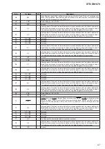
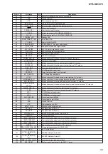
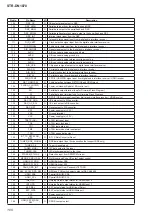
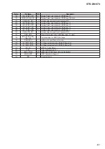
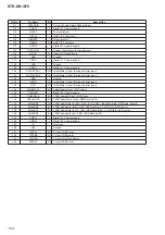
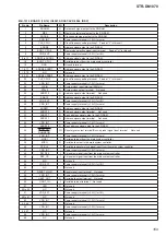
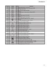
Pin No.
Pin Name
I/O
Description
52
C
I
Regulator stabilization capacity connecting pin
53
VSS
-
Ground terminal
54
VCC
-
Power supply pin (+3.3V)
55
EVOL_DATA
O
Volume data output to BD34702KS2
56
EVOL_CLK
O
I2C clock signal output to the electrical volume
57
INITX
I
Micom input reset port
58
POWER_KEY
I
Power switch input terminal
59
FL_DATA
O
Serial data output for FL DISPLAY DRIVER IC
60
FL_CLK
O
Clock signal output for FL DISPLAY DRIVER IC
61
STANDBY_LED
O
Standby LED
62
PURE_DIRECT_LED
O
Pure Direct LED
63
P_CONT3
O
Power Control for MTK
64
ZONE_SELECT
I
“ZONE SELECT” key input and interrupt
65
V_SEL_SW2
O
Composite video output signal switch
66
NFC_RFDET
I
NFC RF Detect Interrupt and Input
67
NFC_IRQ
I
NFC wireless data reception signal
68
NFC_SDA
O
NFC I2C data input/output
69
NFC_SCL
O
NFC I2C clock signal
70
ZONE2_SPK_RY
O
Relay drive signal (for Zone2) output to Speaker terminal
71
V_SEL_MUTE
O
Composite Video Mute
72
SL_SR_RY
O
Relay drive signal (for surround) output terminal “H”: relay on
73
POWER_RY
O
Relay drive signal (for main power) output terminal “H”: relay on
74
FUSE_DET
I
Fuse open detect signal input
75
AC CUT
I
AC Off detection signal input
76
PROTECT
I
Protect detection signal input terminal
77
BT_TX_MUTE
O
BT TX Rate Converter Mute
78
HP_RY
O
Relay drive signal (for headphone) output terminal “H”: relay on
79
BRIDGEABLE_RY
O
Relay drive signal (for power supply) output terminal “H”: relay on
80
SBL_SBR_RY
O
Relay drive signal (for surround back) output terminal “H”: relay on
81
ZONE2_PREOUT_
SW_RY
O
Relay drive signal (for subwoofer and zone2 preout) output terminal “H”: relay on
82
FRONT_SPK_RY
O
Relay drive signal (for front) output terminal “H”: relay on
83
C_RY
O
Relay drive signal (for center) output terminal “H”: relay on
84
MD1
I
UCOM Mode setting terminal
85
MD0
I
UCOM Mode setting terminal
86
X0(CLOCK IN)
I
Clock signal input (4MHz)
87
X1
O
Clock signal output (4MHz)
88
VSS
-
Ground terminal
89
VCC
-
Power supply pin (+3.3V)
90
INPUT_JOG
I
Function encoder signal input
91
AD_KEY1
I
Key signal input (A/D port)
92
AD_KEY2
I
Key signal input (A/D port)
93
VOLUME_JOG
I
MASTER VOLUME encoder signal input
94
LIMITTER
I
Limiter signal input
95
TEMP_SENSOR2
I
Thermal detection signal input from the thermal sensor
96
TEMP_SENSOR1
I
Thermal detection signal input from the thermal sensor
97
TEMP_SENSOR3
I
Thermal detection signal input from the thermal sensor
98
MODEL
I
Model setting terminal Fixed at “H” in this unit
99
MTK_XPCM_DSD_SEL
O
Chip select signal output for DSD SWAP
100
FS_RATE
I
I2S Fs Rate detect
101
JITTER_REMOVER_
M0
O
NW/DSD Multiplier Select M0
102
JITTER_REMOVER_
M1
O
NW/DSD Multiplier Select M1
103
DSP_SFLASH_HOLD
O
Hold signal output to the serial
fl
ash
104
DSP_RESET
O
System reset signal output to the DSP “L” reset


