124
TA-DA9000ES
Pin No.
Pin Name
I/O
Description
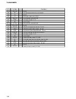
118, 119
GP5, GP4
O
Not used
120
GP3
O
Error signal output to the main system controller
121
NC
—
Not used
122
A0
O
Address signal output to the S-RAM
123 to 125
D4 to D2
I/O
Two-way data bus with the S-RAM
126
VDDE
—
Power supply terminal (+3.3V)
127
VSS
—
Ground terminal
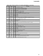
128, 129
D1, D0
I/O
Two-way data bus with the S-RAM
130 to 132
GP2 to GP0
O
Not used
133
SDCLK
O
SD-RAM clock signal output terminal Not used
134
CLKEN
O
SD-RAM chip enable output terminal Not used
135
DQM
O
Output terminal of data input/output mask Not used
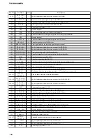
136
EXLOCK
I
Lock signal input from the main system controller
137
VDDI
—
Power supply terminal (+2.6V)
138
VSS
—
Ground terminal
139
MCLK2
O
System clock output terminal (13.5 MHz)
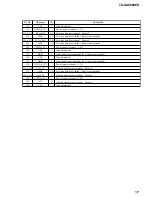
140
PM
I
PLL initialize signal input from the main system controller
141
BST
I
Boot strap signal input from the main system controller
142
BOOT
I
Boot mode control signal input terminal Not used
143
TST
I
Not used
144
MCLK1
I
System clock input terminal (13.5 MHz)


