125
TA-DA9000ES
•
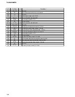
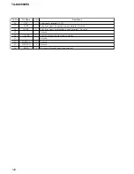
DIGITAL BOARD IC2301 CXD9722TQ (LIP SYNC ADJUST)
Pin No.
Pin Name
I/O
Description
1 to 5
D1 to D5
I/O
Two-way data bus with the SD-RAM
6
VDD
—
Power supply terminal (+3.3V)
7, 8
D6, D7
I/O
Two-way data bus with the SD-RAM
9
VSS
—
Ground terminal
10
WE
O
Write enable signal output to the SD-RAM
11
CAS
O
Column address strobe signal output to the SD-RAM
12
RAS
O
Row address strobe signal output to the SD-RAM
13
CS
O
Chip select signal output to the SD-RAM
14
CLK
O
Clock signal output to the SD-RAM
15
CKE
O
Clock enable signal output to the SD-RAM
16
VDD
—
Power supply terminal (+3.3V)
17 to 22
A11, A10, A0 to A3
O
Address signal output to the SD-RAM
23
VSS
—
Ground terminal
24 to 29
A9 to A4
O
Address signal output to the SD-RAM
30
VSS
—
Ground terminal
31
DRSO
O
Surround R-ch data output terminal Not used
32
DLSO
O
Surround L-ch data output terminal Not used
33
DEXRO
O
Not used
34
DLFEO
O
Sub woofer data output terminal Not used
35
DCO
O
Center data output terminal Not used
36
VDD
—
Power supply terminal (+3.3V)
37
DRO
O
Front R-ch data output terminal Not used
38
DLO
O
Front L-ch data output terminal Not used
39
VSS
—
Ground terminal
40
DMRO
O
Data output terminal for R-ch down mix Not used
41
DMLO
O
Data output terminal for L-ch down mix Not used
42
VSS
—
Ground terminal
43
VDD
—
Power supply terminal (+3.3V)
44
DLDRO
O
Surround back audio data output to the programmable logic device
45
CSWO
O
Center and sub woofer audio data output to the programmable logic device
46
SLSRO
O
Surround audio data output to the programmable logic device
47
FLFRO
O
Front audio data output to the programmable logic device
48
VSS
—
Ground terminal
49
SPDIFO
O
Digital audio data output terminal Not used
50
TEST1
I
Input terminal for the test
51
TRST
I
Reset signal input from terminal Not used
52
TMS
I
Mode selection signal input terminal Not used
53
TCK
I
Clock signal input terminal Not used
54
TDI
I
Serial data signal input terminal Not used
55
TDO
O
Serial data signal output terminal Not used
56
TEST2
I
Input terminal for the test
57
SPDIFI
I
Digital audio data input terminal Not used
58
VSS
—
Ground terminal
59
LRCKI
I
L/R sampling clock signal (44.1 kHz) input from the Dc cut digital filter
60
BCKI
I
Bit clock signal (2.8224 MHz) input from the Dc cut digital filter


