126
TA-DA9000ES
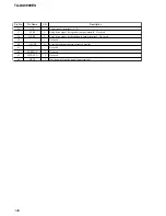
Pin No.
Pin Name
I/O
Description
61
VDD
—
Power supply terminal (+3.3V)
62
VSS
—
Ground terminal
63
DLDRI
I
Surround back audio data input from the Dc cut digital filter
64
CSWI
I
Center and sub woofer audio data input from the Dc cut digital filter
65
SLSRI
I
Surround audio data input from the Dc cut digital filter
66
FLFRI
I
Front audio data input from the Dc cut digital filter
67
TEST3
I
Input terminal for the test
68
CLK512
I
Master clock signal input terminal
69
VSS
—
Ground terminal
70
XRST
I
Reset signal input terminal “L”: reset
71
VDD
—
Power supply terminal (+3.3V)
72
SCLK
I
Serial clock signal input from the main system controller
73
XCS
I
Chip select signal input from the main system controller
74
SI
I
Serial data input from the main system controller
75
SO
O
Serial data output to the main system controller
76
DEXRI
I
Not used
77
DMLI
I
Data input terminal for L-ch down mix Not used
78
DMRI
I
Data input terminal for R-ch down mix Not used
79
VSS
—
Ground terminal
80
PHAI
I
Clock signal input terminal Not used
81
BCKAI
I
Bit clock signal (2.8224 MHz) input terminal Not used
82
DQM
O
Not used
83
DLI
I
Front L-ch data input terminal Not used
84
DRI
O
Front R-ch data input terminal Not used
85
DCI
O
Center data input terminal Not used
86
DLFEI
O
Sub woofer data input terminal Not used
87
DLSI
O
Surround L-ch data input terminal Not used
88
DRSI
O
Surround R-ch data input terminal Not used
89
VSS
—
Ground terminal
90 to 95
D15 to D10
I/O
Two-way data bus with the SD-RAM
96
VDD
—
Power supply terminal (+3.3V)
97, 98
D9, D8
I/O
Two-way data bus with the SD-RAM
99
GND
—
Ground terminal
100
D0
I/O
Two-way data bus with the SD-RAM


