134
TA-DA9000ES
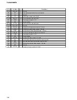
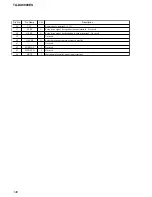
Pin No.
Pin Name
I/O
Description
55, 56
NC
O
Not used
57 to 61
A13 to A9
O
Address signal output to the EEPROM
62
VCC
—
Power supply terminal (+3.3V)
63
A8
O
Address signal output to the EEPROM and i. link interface
64
GND
—
Ground terminal
65 to 71
A7 to A1
O
Address signal output to the EEPROM and i. link interface
72
A0
O
Address signal output terminal Not used
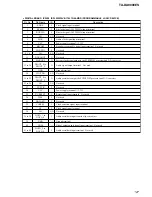
73 to 88
D15 to D0
I/O
Two-way data bus with the EEPROM and i. link interface
89
PHY_BIAS
O
Power down signal output to the i. link interface
90
PHY_RST
O
Power reset signal output to the i. link interface “L”: reset
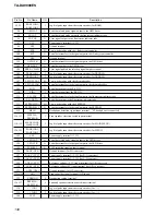
91
NC
O
Not used
92
LINK_RST
O
Link reset signal output to the i. link interface “L”: reset
93 to 95
NC
O
Not used
96
AVSS
—
Ground terminal (for A/D converter)
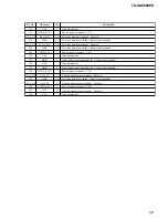
97
NC
O
Not used
98
A/D VREF
I
Reference voltage (+3.3V) input terminal (for A/D converter)
99
AVCC 3.3V
—
Power supply terminal (+3.3V) (for A/D converter)
100
HD7
I/O
Two-way data bus with the i. link DSP


