background image

CHASSIS

SERVICE MANUAL

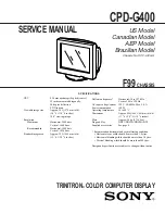
SPECIFICATIONS

CPD-G400

F99

US Model

Canadian Model

AEP Model

Brazilian Model

Chassis No. SCC-L30A-A

TRINITRON

®

 COLOR COMPUTER DISPLAY

CRT

0.24 mm aperture grille pitch (center) 
19 inches measured diagonally 
90-degree deflection
FD Trinitron

Viewable image size

Approx. 365 

×

 274 mm (w/h) 

(14 

3

/

8


×

 10 

7

/

8

 inches) 

18.0" viewing image

Resolution

Maximum

Horizontal: 1800 dots 
Vertical: 1440 lines

Recommended

Horizontal: 1280 dots 
Vertical: 1024 lines

Standard image area

Approx. 352 

×

 264 mm (w/h) 

(13 

7

/

8


×

 10 

1

/

2

 inches)

Deflection frequency*

Horizontal: 30 to 107 kHz
Vertical: 48 to 120 Hz

AC input voltage/current  120 V, 50/60 Hz, Max. 2.0 A
Power consumption

140 W

Operating temperature

10 to 40 ºC

Dimensions

Approx. 446 

×

 464 

×

 461 mm (w/h/d)

(17 

5

/

8

 ×

 18 

3

/

8


×

 18 

1

/

4

 inches)

Mass

Approx. 26 kg (57 lb 5 oz)

Plug and Play

DDC1/DDC2B/DDC2Bi/GTF 

Supplied accessories

See page 6

* Recommended horizontal and vertical timing condition

• Horizontal sync width should be more than 1.0 

µ

sec.

• Horizontal blanking width should be more than 3.0 

µ

sec.

• Vertical blanking width should be more than 500 

µ

sec.

Design and specifications are subject to change without notice.

Summary of Contents for TRINITRON CPD-G400

Page 1: ...mage area Approx 352 264 mm w h 13 7 8 10 1 2 inches Deflection frequency Horizontal 30 to 107 kHz Vertical 48 to 120 Hz AC input voltage current 120 V 50 60 Hz Max 2 0 A Power consumption 140 W Operating temperature 10 to 40 ºC Dimensions Approx 446 464 461 mm w h d 17 5 8 18 3 8 18 1 4 inches Mass Approx 26 kg 57 lb 5 oz Plug and Play DDC1 DDC2B DDC2Bi GTF Supplied accessories See page 6 Recomme...

Page 2: ...POSANTS IDENTIFIÉS PAR UNE TRAME ET UNE MARQUE SONT CRITIQUES POUR LA SÉCURITÉ NE LES REMPLACER QUE PAR UNE PIÈCE PORTANT LE NUMÉRO SPECIFIÉ LES RÉGLAGES DE CIRCUIT DONT L IMPORTANCE EST CRITIQUE POUR LA SÉCURITÉ DU FONCTIONNEMENT SONT IDENTIFIÉS DANS LE PRÉSENT MANUEL SUIVRE CES PROCÉDURES LORS DE CHAQUE REMPLACEMENT DE COMPOSANTS CRI TIQUES OU LORSQU UN MAUVAIS FONCTIONNE MENT EST SUSPECTÉ After...

Page 3: ... orange If the 1 power indicator is lit in orange the computer is in power saving mode Try pressing any key on the keyboard If the 1 power indicator is green 1 Disconnect the video input cable or turn off the connected computer 2 Press the 1 power button twice to turn the monitor off and then on 3 Move the control button for 2 seconds before the monitor enters power saving mode If all four color b...

Page 4: ...67 H BLK 5 720 2 440 2 765 H FP 0 318 0 279 0 316 H SYNC 3 813 0 837 0 948 H BP 1 589 1 325 1 501 H ACTIV 26 057 6 972 7 901 VERTICAL V FREQ HZ 70 087 Hz 85 000 Hz 75 000 Hz lines lines lines V TOTAL 449 1250 1250 V BLK 35 50 50 V FP 5 1 1 V SYNC 2 3 3 V BP 28 46 46 V ACTIV 414 1200 1200 SYNC INT G NO NO NO EXT H V POLARITY YES N P YES P P YES P P EXT CS POLARITY NO NO NO INT NON INT NON INT NON I...

Page 5: ...be Removal 2 4 2 8 Harness Location 2 5 3 SAFETY RELATED ADJUSTMENT 3 1 4 ADJUSTMENTS 4 1 5 DIAGRAMS 5 1 Block Diagrams 5 1 5 2 Frame Schematic Diagram 5 5 5 3 Circuit Boards Location 5 6 5 4 Schematic Diagrams and Printed Wiring Boards 5 7 1 Schematic Diagram of A Board 5 9 2 Schematic Diagrams of D a b c Board 5 11 3 Schematic Diagrams of N H Boards 5 19 5 5 Semiconductors 5 21 6 EXPLODED VIEWS ...

Page 6: ...abrasive pad scouring powder or solvent such as alcohol or benzene Transportation When you transport this monitor for repair or shipment use the original carton and packing materials Use of the tilt swivel This monitor can be adjusted within the angles shown below To find the center of the monitor s turning radius align the center of the monitor s screen with the centering dots on the stand Hold t...

Page 7: ...to adjust the picture If no picture appears on your screen Check that the monitor is correctly connected to the computer If NO INPUT SIGNAL appears on the screen confirm that the video signal cable is properly connected and all plugs are firmly seated in their sockets If MONITOR IS IN POWER SAVE MODE appeared on the screen try pressing any key on the computer keyboard If you are replacing an old m...

Page 8: ...button to display the main MENU on your screen See page 10 for more information on using the control button Use the control button to select one of the following menus x Displaying the current input signal The horizontal and vertical frequencies of the current input signal are displayed in the main MENU If the signal matches one of this monitor s factory preset modes the resolution is also display...

Page 9: ...e control button m M to select AUTO Then move the control button The picture automatically fills the screen Notes This function is intended for use with a computer running Windows or similar graphic user interface software that provides a full screen picture It may not work properly if the background color is dark or if the input picture does not fill the screen to the edges such as an MS DOS prom...

Page 10: ... the picture sides to the left or right adjust the picture width at the top of the screen shift the picture to the left or right at the top of the screen 9 3 0 0K 5 0 0 0K 2 6 COLOR sRGB 9 3 0 0K 5 0 0 0K OFF ON COLOR sRGB 13 US Adjusting the convergence CONV The CONV settings allow you to adjust the quality of the picture by controlling the convergence The convergence refers to the alignment of t...

Page 11: ... too large for the screen adjust the resolution to the figures shown in the menu using your computer If the input signal matches one of this monitor s factory preset modes the resolution and refresh rate of the current input signal are displayed FLICKER If the picture is flickering adjust the refresh rate to figures shown in the menu If the input signal matches one of this monitor s factory preset...

Page 12: ...computer or other equipment please refer to the connected equipment s instruction manual Use the self diagnosis function page 19 if the following recommendations do not resolve the problem Symptom Check these items No picture If the 1 power indicator is not lit Check that the power cord is properly connected Check that the 1 power switch is in the on position If the NO INPUT SIGNAL message appears...

Page 13: ...T I ON MENU MODEL CPD G4 0 0 SER NO 1 2 3 4 5 6 7 MANUFACTURED 1 9 9 I NFORMAT I ON 9 5 2 Example b 19 US Self diagnosis function This monitor is equipped with a self diagnosis function If there is a problem with your monitor or computer the screen will go blank and the 1 power indicator will either light up green or flash orange If the 1 power indicator is lit in orange the computer is in power s...

Page 14: ...3 Cabinet Push in the tip of a screwdriver about 5mm to unlock the four cloaws 1 Two claws Two claws 2 Two screws BVTP 4 x 16 Bezel assembly Cabinet Cabinet 5 Four screws BVTT 4 x 8 7 Three screws BVTT 4 x 8 8 Video shield 3 Two screws BVTT 4 x 8 1 2 EMI shield Upper 4 Side cover L 6 Side cover R Three screws BVTT 4 x 8 ...

Page 15: ...VTT 4 x 8 2 Cable stopper 3 Two screws 5 Three screws BVTT 3 x 8 CN601 CN600 CN303 8 D board N board 6 Screw P 3 5 x 20 7 Two screws BVTP 3 x 8 2 Screw BVTT 4 x 8 4 Rear shield complete assembly 1 Cable cover 3 Widening the chassis toward the direction A disengage two claws A A Refering to 2 3 disconnect five connectors CN303 CN305 CN306 CN309 and CN311 ...

Page 16: ...TP 4 x 16 Bezel assembly Two H printed circuit board brackets Menu button Input selection CN801 Picture tube shield Before removing the bezel assembly secure the picture tube shield at the positions shown with the arrow diagonal two places to prevent the picture tube from falling Use the screws BVTT 4 8 that fix shield 7 3 6 8 5 4 2 1 ...

Page 17: ...sharp shaped material 2 Don t press the rubber hardly not to damage inside of anode caps A material fitting called as shatter hook terminal is built in the rubber 3 Don t turn the foot of rubber over hardly The shatter hook terminal will stick out or damage the rubber REMOVAL OF ANODE CAP NOTE Short circuit the anode of the picture tube and the anode cap to the metal chassis CRT shield or carbon p...

Page 18: ...5 CN603 CN501 CN600 H board Degaussing coil N board FBT A board Picture tube Rear shield Side cover L CN11 CN2001 CN1 CN702 CN701 CN904 CN601 CN315 CN309 CN301 CN313 CN302 CN1003 CN1002 CN1004 D board AC inlet CN310 CN306 CN311 CN303 ...

Page 19: ...tween 200 V Line and GND and make sure that OCP will function Power LED will vanish and the sound chi chi chi will be heard and cut off AC input promptly e Power Supply Operation Check 1 Apply AC100 V to the D Board 2 Make sure that the line voltage at the both ends of C621 is 200 3 0 VDC HV Regulator Circuit Check HV Protector Circuit Check Beam Current Protector Circuit Check When replacing or r...

Page 20: ...ed before assembling the chassis 7 Perform auto degaussing 8 Attach the wobbling coil to the designated part of the CRT neck 9 Attach the sensor of the landing adjustment unit on the CRT surface 10 Adjust the DY position and purity and the DY tilt Note Use purity magnet on the DY 11 Fasten DY with screw Note Torque 22 2 kg cm 2 2 0 2 Nm 12 Perform auto degaussing 13 Using two wedges adjust vertica...

Page 21: ...ach magnet and TLH plate a Align the protrusion marked with an arrow White Balance Adjustment Specification 1 9300 K x 0 283 0 005 y 0 298 0 005 All White 2 5000 K x 0 346 0 005 y 0 359 0 005 All White 3 sRGB x 0 313 0 005 y 0 329 0 005 All White Vertical and Horizontal Position and Size Specification Focus adjustment Adjust the focus volume 1 and 2 for the optimum focus Convergence Specification ...

Page 22: ...2 RGB OUT IC004 RGB CUT OFF CONT IC007 DDC 13 2 3 14 1 12 15 13 12 3 14 15 1 2 INPUT1 INPUT2 A B 7 3 5 IC006 INVERTER 1 14 2 3 4 1 2 1KV 1KV CN301 D 7 H1 CN305 G2 C BLOCK G2 HC FC TO FBT FV C KB KR KG HEATER G2 CONT Q001 IC005 G2 CUT OFF CONT BUFF Q005 BUFF Q004 TEST19 PC1 FIL Q804 SYNC SEPALATOR Q002 003 V901 PICTURE TUBE 5 11 7 3 2 4 15 7 13 14 6 V SYNCO C BLK DSP RESET IIC SDA IIC SCL H SYNCO H...

Page 23: ...REG SW Q901 200V BUFF Q507 H CENT Q517 519 STBY 5V 6 5 1 7 5 3 6 1 9 5 4 7 SCL SDA S CAP CANGE Q511 516 OSCONT OSCIN WC IC1005 ROM OUT IC607 IC401 V OUT 1 1 2 2 3 9 8 7 5 3 2 18 17 16 15 5 1 3 4 2 14 13 12 11 10 1 4 3 3 2 4 2 1 7 7 6 14 11 12 18 10 3 1 5 6 12V H LIN BAL SW Q510 REF 9V 1 4 DGC DGC CN610 1 2 3 AC L NC AC H CN600 F601 S601 D625 AC RECT 15V TH600 TH601 RY601 RY602 LF602 LFT AC IN DGC ...

Page 24: ... NC NC AC L AC H NC 80V GND H1 12V GND 200V H SYNCO V SYNCO GND 5V 2 INPUT SEL C SYNC V SYNC H SYNC NC 1KV INPUT SEL INPUT SEL GND C BLK STBY 5V BP CLP DDC SCL DDC SDA IIC SDA IIC SCL H FBP GND CPU GND1 CPU GND2 H SYNCO V SYNCO GND 5V 2 INPUT SEL C SYNC V SYNC H SYNC GND C BLK STBY 5V BP CLP DDC SCL DDC SDA IIC SDA IIC SCL H FBP TO CRT SHIELD USER CONTROL AC IN POWER H DEF HV TO ECS V DY H DY ROTA...

Page 25: ... D board circuit diagram is divided into three sheets each having the code D a to D c For example the destination ab1 on the code D a sheet is connected to ab1 on the D b sheet a b 1 Ref No Circuit diagram division code HV ADJ Part Replaced RV901 HV Regulator Circuit Check HV Protector Circuit Check Beam Current Protector Circuit Check Part Replaced D Board T901 FBT IC901 R924 R925 RV901 Mounted D...

Page 26: ...S119 1k CHIP 0 1 25V B CHIP 0 1 25V B CHIP 270k CHIP 1k CHIP 0 1 25V B CHIP 0 1 25V B CHIP 270k CHIP 1k CHIP 0 1 25V B CHIP 270k CHIP 0 1 25V B CHIP 0 1 25V B CHIP 0 1 25V B CHIP 0 1 250V 10 250V 0 1 25V B CHIP 0 47 250V 0 47 250V 470k CHIP 470k CHIP 470k CHIP 470k CHIP 470k CHIP 470k CHIP 0 47 250V 0 1 100V 8 2k CHIP 0 022 B CHIP 8 2k CHIP 0 022 B CHIP 0 1 25V B CHIP 100 CHIP 100 CHIP 220µH 470k ...

Page 27: ...22k CHIP 2 2k CHIP 1k CHIP 1k CHIP 8 2k CHIP 220 CHIP 220 CHIP 220 CHIP 1k CHIP 1k CHIP 100 CHIP 100 CHIP 10k CHIP 0 22 100V PT 0 01 50V B CHIP 0 1 25V F CHIP 15P 1k CHIP 100 CHIP 220 CHIP 220 CHIP 8P WHT S MICRO 4 7 1W RS 4P WHT 0 CHIP 0 CHIP 10k RN CP 100k 1 2W RC 4 7k RN 3300p B CHIP 22 15k RN 10k CHIP 47k CHIP 8P WHT S MICRO 10000p B CHIP 0 CHIP 3 3k RN CP 33k CHIP 100 CHIP 4700p B CHIP 4700p ...

Page 28: ... FPRD 100 FPRD 100 FPRD 100 FPRD 100 FPRD 9 1k RN CP 4 7k RN CP 10k 10k CHIP 22k CHIP 100 CHIP 0 0022 100V PT 100p 2kV SL 4 7 250V 2200 25V 1000 25V HR 2 7k RN CP 2 7k RN CP 10k RN CP 120 1 2W RN 120 1 2W RN 1000 25V HLC 100 100V 47 25V 4 7mH 470 16V 220 25V ERA91 02TP1 HDT 4 7M 1 2W SURGE 0 47 1W RS 47k 2W RS 47k 2W RS 10k 3W RS UDZ TE 17 15B 680p 2kV 120 1 2W RN 0 1 B CHIP JW 5 47 1W RS 0 0047 M...

Page 29: ... C910 C911 C912 D901 D903 D904 C902 C925 C926 SG901 C927 R925 C520 R526 C523 R527 R528 R530 D509 R532 C515 R531 C522 D507 D508 R529 R904 C917 R522 R912 R914 R523 D512 R538 C528 R537 R535 D511 R533 C530 C918 C527 C551 C517 C525 C558 R698 R697 FB502 D915 R934 D705 C914 FB901 D906 D907 D909 C915 C916 CN501 R930 R931 R933 R917 D911 D910 R923 R920 R919 R918 C920 C901 C909 R906 R902 R901 C903 D913 R926 ...

Page 30: ... 18 D BOARD D µ COM POWER DEFLECTION 1 A B C D E 2 3 4 5 6 7 NOTE The circuit indicated as left contains high voltage of over 600 Vp p Care must be paid to prevent an electric shock in inspection or repairing ...

Page 31: ... 25V F CHIP 0 1 25V F CHIP 0 1 25V F CHIP 0 022 B CHIP 12k RN CP 12k RN CP 1k RN CP 1k CHIP 180 CHIP 470k RN CP 4 7k RN CP 6 8k RN CP 6 8k RN CP 4 7k RN CP 47 25V 470 6 3V 47 25V 470 6 3V 470 6 3V 47 25V 220 CHIP CHIP 10k CHIP 1k CHIP 10k CHIP 100 CHIP 100 CHIP 10k RN CP 4 7k CHIP 1 5k CHIP 0 CHIP 0 047 25V B CHIP 4700p B CHIP 4700p B CHIP 4700p B CHIP 2SC2412K 220k CHIP 2SA1037K 680k CHIP 100 CHI...

Page 32: ...n SOP 1 TOP VIEW n 8 pin SOP 1 TOP VIEW n 16 pin SOP 1 TOP VIEW n CXD9517Q CXD9522S CXD9523S JCN Ver 1 2 ST92T175N1B1 JCJ LA6510 LM324M LA78040 LM2402T 24 pin DIP 64 pin QFP 1 TOP VIEW n 1 TOP VIEW n 56 pin DIP 1 TOP VIEW n 10 1 7 1 14 pin SOP 1 TOP VIEW n 32 pin DIP 1 TOP VIEW n 36 pin SOP 1 TOP VIEW n 1234 1 2 3 TEA1504 N2 DTC144ESA TP PDTC114 EK 115 2SA1049 GR 2SA1049TP GR FS5KM 16A FS5KM 18A A...

Page 33: ... G12S FMQ G5FMS PG124S15 YG911S2R D4SB60L D4SB60L F EGP10D EGP10GPKG23 ERA91 02 ERA91 02TP1 RH 1A CATHODE ANODE 1 2 1 2 CATHODE ANODE EGP10DPKG23 HZS182 TE HZS9 1NB2 MTZJ T 77 15B MTZJ 6 2B MTZJ T 77 4 7B MTZJ T 77 6 2 RD10ES T1B2 RD10ESB2 RD15ES B2 RD16ES B3 RD16ES T1B2 RD18ES B2 RD18ESB RD4 7ES T1B2 RD4 7ESB2 RD5 1ES B2 RD5 1ES T1B2 RD5 6ESB2 RD8 2ES B2 RD8 2ES T1B2 RD9 1ES T1B2 1SS119 25 1SS119...

Page 34: ...VIEWS The components identified marked are critical for safety Replace only with the part number specified Les composants identifiés par la marque sont critiques pour la sécurité Ne les remplacer que par une pièce portant le numéro spécifié 10 11 1 12 2 13 3 4 5 6 7 8 9 1 4 071 715 12 COVER CABLE 2 4 394 972 21 CAP POWER 3 A 1346 879 B D BOARD COMPLETE U C 4 5 3 A 1346 880 B D BOARD COMPLETE AEP 4...

Page 35: ...X12 BV TAP 56 4 044 932 11 EMBLEM NO 8 SONY 57 4 070 217 01 CUSHION 58 4 060 359 01 HOLDER PRINTED CIRCUIT BOARD 59 0 8 736 407 61 ITC ASSY 19TKC R1 AEP U C 60 62 59 0 8 736 408 61 ITC ASSY 19TKC RS1 BRZ 60 62 60 0 8 451 284 11 DEFLECTION YOKE Y19TKK V 61 0 1 452 912 61 NECK ASSEMBLY NA 2914 62 2 162 100 21 SPACER DEFLECTION YOKE 63 4 047 316 01 SPRING EXTENSION 64 0 1 419 285 11 COIL DEGAUSSING 6...

Page 36: ...N BRZ 102 4 072 843 01 CUSHION LOWER ASSY U C 102 4 072 902 01 CUSHION LOWER ASSY AEP 102 4 074 997 01 CUSHION LOWER ASSY BRZ 103 4 072 842 01 CUSHION UPPER ASSY U C 103 4 072 902 01 CUSHION UPPER ASSY AEP 103 4 074 994 01 CUSHION UPPER ASSY BRZ 104 4 041 927 31 BAG POLYETHYLENE 105 1 793 504 11 CABLE ASSY 15P DSUB X2 CONNECTOR 106 0 1 765 719 31 CORD SET POWER AEP 106 0 1 790 662 11 CORD SET POWE...

Page 37: ...IC 0 001uF 10 500V C032 1 164 004 11 CERAMIC CHIP 0 1uF 10 25V C033 1 164 004 11 CERAMIC CHIP 0 1uF 10 25V C035 1 162 134 11 CERAMIC 470pF 10 2KV C037 1 101 006 00 CERAMIC 0 047uF 50V C038 1 163 009 11 CERAMIC CHIP 0 001uF 10 50V C039 1 165 319 11 CERAMIC CHIP 0 1uF 50V C040 1 163 021 91 CERAMIC CHIP 0 01uF 10 50V C041 1 162 318 11 CERAMIC 0 001uF 10 500V C042 1 165 319 11 CERAMIC CHIP 0 1uF 50V C...

Page 38: ... 062 51 DIODE 1PS226 115 D104 8 719 052 12 DIODE 1SS376TE 17 D104 8 719 052 12 DIODE 1SS376TE 17 D105 8 719 052 12 DIODE 1SS376TE 17 D105 8 719 052 12 DIODE 1SS376TE 17 D106 8 719 052 12 DIODE 1SS376TE 17 D106 8 719 052 12 DIODE 1SS376TE 17 D108 8 719 062 51 DIODE 1PS226 115 D109 8 719 052 12 DIODE 1SS376TE 17 D109 8 719 052 12 DIODE 1SS376TE 17 D111 8 719 062 51 DIODE 1PS226 115 D201 8 719 062 51...

Page 39: ...216 296 91 SHORT 0 JR032 1 216 296 91 SHORT 0 JR033 1 216 296 91 SHORT 0 COIL L004 1 412 529 11 INDUCTOR 22uH L005 1 412 537 31 INDUCTOR 100uH L006 1 412 541 41 INDUCTOR 220uH L007 1 408 615 31 INDUCTOR 100uH TRANSISTOR Q001 8 729 032 61 TRANSISTOR 2SC5022 02 Q002 8 729 216 22 TRANSISTOR 2SA1162 G Q003 8 729 216 22 TRANSISTOR 2SA1162 G Q004 8 729 216 22 TRANSISTOR 2SA1162 G Q005 8 729 216 22 TRANS...

Page 40: ... R120 1 216 113 00 RES CHIP 470K 5 1 10W R122 1 216 113 00 RES CHIP 470K 5 1 10W R123 1 216 037 00 RES CHIP 330 5 1 10W R130 1 216 019 00 RES CHIP 56 5 1 10W R133 1 216 019 00 RES CHIP 56 5 1 10W R140 1 216 019 00 RES CHIP 56 5 1 10W R151 1 219 742 11 CARBON 47 5 1 2W R161 1 215 395 00 METAL 82 1 1 4W R201 1 215 395 00 METAL 82 1 1 4W R204 1 216 009 91 RES CHIP 22 5 1 10W R206 1 216 071 00 RES CHI...

Page 41: ... 038 91 CERAMIC CHIP 0 1uF 25V C535 1 164 004 11 CERAMIC CHIP 0 1uF 10 25V C536 1 107 665 11 ELECT 0 47uF 20 400V C537 1 107 770 11 FILM 0 16uF 3 400V C538 1 107 651 11 ELECT 4 7uF 20 250V C539 1 117 673 11 FILM 1 5uF 5 250V C540 1 107 888 11 ELECT 47uF 20 25V C541 1 109 844 11 FILM 0 68uF 5 250V C542 1 163 021 91 CERAMIC CHIP 0 01uF 10 50V C543 1 117 665 11 FILM 0 33uF 5 250V C544 1 163 021 91 CE...

Page 42: ...IP 0 1uF 10 50V C905 1 163 133 00 CERAMIC CHIP 470pF 5 50V C906 1 163 251 11 CERAMIC CHIP 100pF 5 50V C907 1 163 275 11 CERAMIC CHIP 0 001uF 5 50V C908 1 164 505 11 CERAMIC CHIP 2 2uF 16V C909 1 104 665 11 ELECT 100uF 20 25V C910 1 163 259 91 CERAMIC CHIP 220pF 5 50V C911 1 163 243 11 CERAMIC CHIP 47pF 5 50V C912 1 163 021 91 CERAMIC CHIP 0 01uF 10 50V C913 1 119 748 11 ELECT 33uF 20 400V C914 1 1...

Page 43: ... 42 DIODE 1N4148S 26TP D703 8 719 061 42 DIODE 1N4148S 26TP D705 8 719 158 49 ZENER DIODE RD12SB2 D901 8 719 073 01 DIODE MA111 K8 S0 D903 8 719 073 01 DIODE MA111 K8 S0 D904 8 719 073 01 DIODE MA111 K8 S0 D906 8 719 978 65 ZENER DIODE DTZ TT11 15B D907 8 719 052 86 DIODE D2L40 TA D908 8 719 073 01 DIODE MA111 K8 S0 D909 8 719 978 65 ZENER DIODE DTZ TT11 15B D910 8 719 028 72 DIODE RGP02 17EL 6433...

Page 44: ...NEARITY L503 1 419 298 11 COIL HORIZONTAL CENTER L504 1 406 675 11 INDUCTOR 4 7mH L505 1 406 675 11 INDUCTOR 4 7mH L506 1 406 675 11 INDUCTOR 4 7mH L507 1 412 537 31 INDUCTOR 100uH L603 1 412 537 31 INDUCTOR 100uH L604 1 406 665 11 INDUCTOR 100uH L606 1 406 665 11 INDUCTOR 100uH L607 1 414 158 11 INDUCTOR 2 2uH L608 1 414 487 41 INDUCTOR 1uH L901 1 412 537 31 INDUCTOR 100uH L902 1 406 659 11 INDUC...

Page 45: ...1 1 216 687 11 METAL CHIP 33K 0 50 1 10W R542 1 214 842 11 METAL 120 1 1 2W R543 1 214 842 11 METAL 120 1 1 2W R544 1 249 393 11 CARBON 10 5 1 4W F R545 1 216 057 00 RES CHIP 2 2K 5 1 10W R546 1 215 909 11 METAL OXIDE 47 5 3W F R547 1 215 387 00 METAL 39 1 1 4W R548 1 260 318 71 CARBON 150 5 1 2W R549 1 260 314 11 CARBON 68 5 1 2W R550 1 247 903 00 CARBON 1M 5 1 4W R552 1 249 437 11 CARBON 47K 5 1...

Page 46: ... 15 5 1W F R714 1 215 863 11 METAL OXIDE 100 5 1W F R715 1 216 353 00 METAL OXIDE 2 2 5 1W F R716 1 249 377 11 CARBON 0 47 5 1 4W F R717 1 249 377 11 CARBON 0 47 5 1 4W F R718 1 216 426 11 METAL OXIDE 82 5 1W F R719 1 216 369 00 METAL OXIDE 1 5 2W F R720 1 216 295 91 SHORT 0 R721 1 216 659 11 METAL CHIP 2 2K 0 50 1 10W R722 1 216 426 11 METAL OXIDE 82 5 1W F R723 1 216 295 91 SHORT 0 R724 1 216 65...

Page 47: ...216 065 91 RES CHIP 4 7K 5 1 10W R1073 1 216 049 91 RES CHIP 1K 5 1 10W R1074 1 216 049 91 RES CHIP 1K 5 1 10W R1083 1 216 025 91 RES CHIP 100 5 1 10W R1084 1 216 041 00 RES CHIP 470 5 1 10W R1085 1 216 025 91 RES CHIP 100 5 1 10W R1086 1 216 073 00 RES CHIP 10K 5 1 10W R1092 1 216 033 00 RES CHIP 220 5 1 10W R1093 1 216 033 00 RES CHIP 220 5 1 10W R1094 1 216 113 00 RES CHIP 470K 5 1 10W R1095 1 ...

Page 48: ...R802 1 216 677 11 METAL CHIP 12K 0 50 1 10W R803 1 216 033 00 RES CHIP 220 5 1 10W R804 1 216 033 00 RES CHIP 220 5 1 10W R805 1 216 033 00 RES CHIP 220 5 1 10W R806 1 216 033 00 RES CHIP 220 5 1 10W R807 1 216 033 00 RES CHIP 220 5 1 10W R808 1 216 033 00 RES CHIP 220 5 1 10W R809 1 216 651 11 METAL CHIP 1K 0 50 1 10W R810 1 216 651 11 METAL CHIP 1K 0 50 1 10W R811 1 216 057 00 RES CHIP 2 2K 5 1 ...

Page 49: ... 911 31 FERRITE 1 1uH FB2002 1 412 911 31 FERRITE 1 1uH FB2003 1 412 911 31 FERRITE 1 1uH FB2004 1 412 911 31 FERRITE 1 1uH FB2005 1 412 911 31 FERRITE 1 1uH TRANSISTOR Q2001 8 729 119 76 TRANSISTOR 2SA1175 HFE Q2002 8 729 119 76 TRANSISTOR 2SA1175 HFE RESISTOR R2001 1 249 422 11 CARBON 2 7K 5 1 4W R2002 1 249 429 11 CARBON 10K 5 1 4W R2003 1 249 429 11 CARBON 10K 5 1 4W R2004 1 215 411 00 METAL 3...

Page 50: ...y with the part number specified Les composants identifiés par la marque sont critiques pour la sécurité Ne les remplacer que par une pièce portant le numéro spécifié CPD G400 7 14 Sony Corporation Computer Display Company Computer Display DIV 9 978 652 01 CPD G400 9 978 652 01 99JL05252 1 62 English 99JL05252 1 Printed in Japan 1999 10 ...

Reviews: