1-12
IC
VGN-
S36C/S36GP/S36LP/S36SP/S36TP/S38CP/
S52B/
S62PS/S62PSY/S62S/
S350F/S350FP/
S360/S360P/
S370F
(J/AM
/AO
)
Confidential
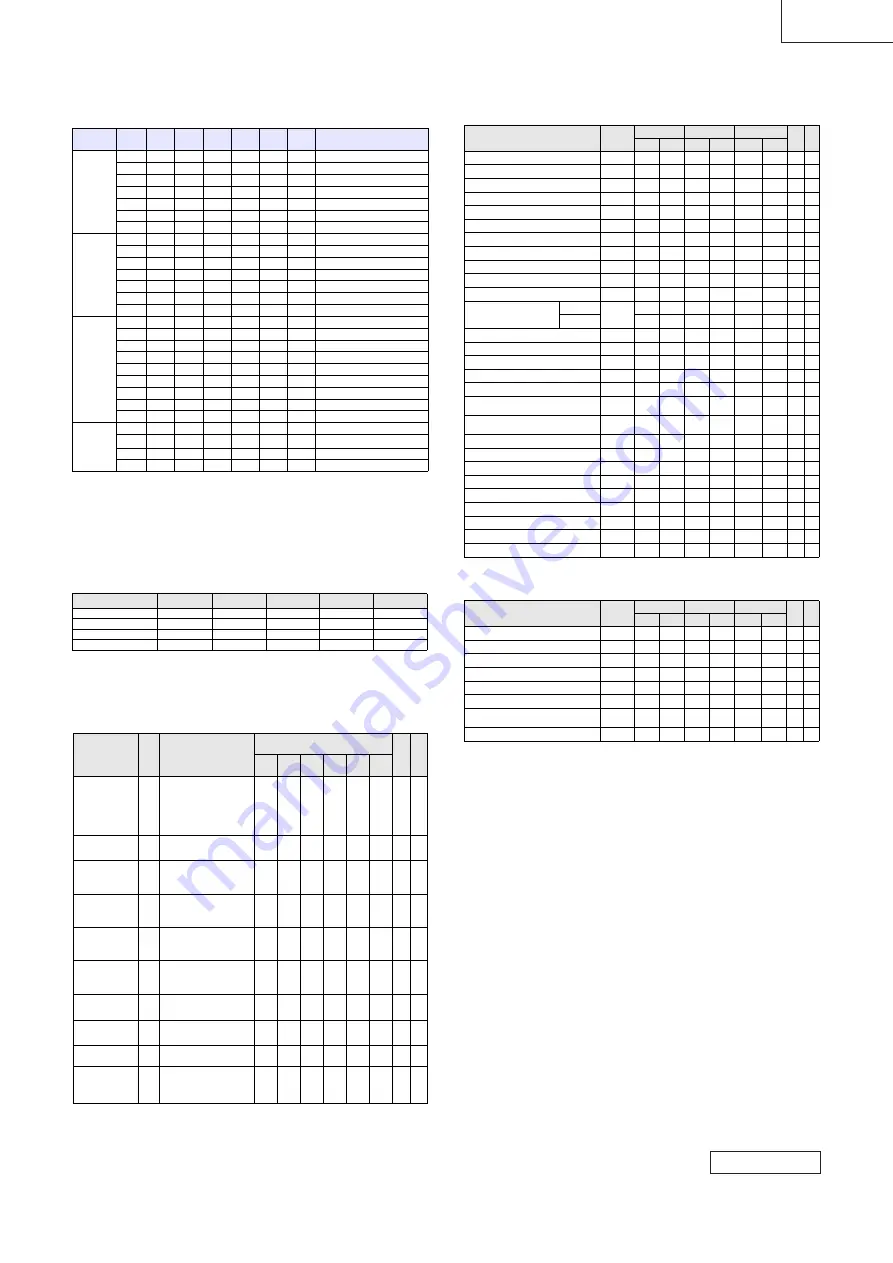
CKE FUNCTION TRUTH TABLE
Note :
When CKE=L, all DQ and DQS(0~3) must be in Hi-Z state.
1. CKE and /CS must be kept high for a minimum of 200 stable input clocks before issuing any command.
2. All command can be stored after 2 clocks from low to high transition of CKE.
3. Illegal if CK is suspended or stopped during the power down mode.
4. Self refresh can be entered only from the all banks idle state.
5. Disabling CK may cause malfunction of any bank which is in active state.
Current
State
CKEn-
1
CKEn
/CS
/RAS
/CAS
/WE
/ADD
Action
SELF
REFRESH
1
H
X
X
X
X
X
X
INVALID
L
H
H
X
X
X
X
Exit self refresh, enter idle after tSREX
L
H
L
H
H
H
X
Exit self refresh, enter idle after tSREX
L
H
L
H
H
L
X
ILLEGAL
L
H
L
H
L
X
X
ILLEGAL
L
H
L
L
X
X
X
ILLEGAL
L
L
X
X
X
X
X
NOP, continue self refresh
POWER
DOWN
2
H
X
X
X
X
X
X
INVALID
L
H
H
X
X
X
X
Exit power down, enter idle
L
H
L
H
H
H
X
Exit power down, enter idle
L
H
L
H
H
L
X
ILLEGAL
L
H
L
H
L
X
X
ILLEGAL
L
H
L
L
X
X
X
ILLEGAL
L
L
X
X
X
X
X
NOP, continue power down mode
ALL BANKS
IDLE
4
H
H
X
X
X
X
X
See operation command truth table
H
L
L
L
L
H
X
Enter self refresh
H
L
H
X
X
X
X
Exit power down
H
L
L
H
H
H
X
Exit power down
H
L
L
H
H
L
X
ILLEGAL
H
L
L
H
L
X
X
ILLEGAL
H
L
L
L
H
X
X
ILLEGAL
H
L
L
L
L
L
X
ILLEGAL
L
L
X
X
X
X
X
NOP
ANY STATE
OTHER
THAN
ABOVE
H
H
X
X
X
X
X
See operation command truth table
H
L
X
X
X
X
X
ILLEGAL
5
L
H
X
X
X
X
X
INVALID
L
L
X
X
X
X
X
INVALID
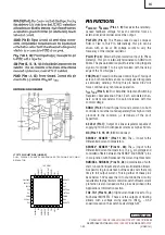
DC CHARACTERISTICS I
(TA=0 to 70
o
C, Voltage referenced to V
SS
= 0V)
Note
:
1. V
IN
= 0 to 3.6V, All other pins are not tested under V
IN
=0V. 2. D
OUT
is disabled, V
OUT
=0 to 2.7V
Parameter
Symbol
Min
Max
Unit
Note
Input Leakage Current
I
LI
-2
2
uA
1
Output Leakage Current
I
LO
-5
5
uA
2
Output High Voltage
V
OH
V
TT
+ 0.76
-
V
I
OH
= -15.2mA
Output Low Voltage
V
OL
-
V
TT
- 0.76
V
I
OL
= +15.2mA
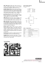
DC CHARACTERISTICS II
(TA=0 to 70
o
C, Voltage referenced to V
SS
= 0V)
Note :
1. I
DD1, IDD4
and I
DD5
depend on output loading and cycle rates. Specified values are measured with the output open.
2. Min. of t
RFC
(Auto Refresh Row Cycle Time) is shown at AC CHARACTERISTICS.
Parameter
Sym
bol
Test Condition
Speed
Unit
Note
2
22
25
28
33
36
Operating Current
I
DD0
One bank; Active - Precharge;
tRC=tRC(min); tCK=tCK(min);
DQ,DM and DQS inputs changing
twice per clock cycle; address and
control inputs changing once per
clock cycle
230
210
190
180
170
160
mA
1
Operating Current
I
DD1
Burst length=2, One bank active
t
RC
t
t
RC
(min), I
OL
=0mA
250
230
210
200
190
180
mA
1
Precharge Standby
Current in Power Down
Mode
I
DD2P
CKE
d
V
IL
(max), t
CK
=min
45
40
35
30
25
25
mA
Precharge Standby
Current in Non Power
Down Mode
I
DD2N
CKE
t
V
IH
(min), /CS
t
V
IH
(min),
t
CK
= min, Input signals are
changed one time during 2clks
140
130
120
110
100
90
mA
Active Standby Cur-
rent in Power Down
Mode
I
DD3P
CKE
d
V
IL
(max), t
CK
=min
50
45
40
35
30
30
mA
Active Standby Cur-
rent in Non Power
Down Mode
I
DD3N
CKE
t
V
IH
(min), /CS
t
V
IH
(min),
t
CK
=min, Input signals are
changed one time during 2clks
190
170
150
130
115
110
mA
Burst Mode Operating
Current
I
DD4
t
CK
t
t
CK
(min), I
OL
=0mA
All banks active
750
700
650
590
500
450
mA
1
Auto Refresh Current
I
DD5
t
RC
t
t
RFC
(min),
All banks active
400
400
350
350
300
300
mA
1,2
Self Refresh Current
I
DD6
CKE
d
0.2V
3
3
3
3
3
3
mA
Operating Current -
Four Bank Operation
I
DD7
Four bank interleaving with BL=4,
Refer to the following page for
detailed test condition
1100
1000
900
800
700
600
mA
AC CHARACTERISTICS - I
(AC operating conditions unless otherwise noted)
Parameter
Symbol
2
22
25
Unit
Note
Min
Max
Min
Max
Min
Max
Row Cycle Time
t
RC
23
-
21
-
18
-
CK
Auto Refresh Row Cycle Time
t
RFC
26
-
24
-
21
-
CK
Row Active Time
t
RAS
16
120K
14
120K
12
120K
CK
Row Address to Column Address Delay for Read
t
RCDRD
7
-
7
-
6
-
CK
Row Address to Column Address Delay for Write
t
RCDWR
4
-
3
-
3
-
CK
Row Active to Row Active Delay
t
RRD
4
-
4
-
4
-
CK
Column Address to Column Address Delay
t
CCD
2
-
2
-
1
-
CK
Row Precharge Time
t
RP
7
-
7
-
6
-
CK
Write Recovery Time
t
WR
4
-
4
-
3
-
CK
Last Data-In to Read Command
t
DRL
2
-
2
-
2
-
CK
Auto Precharge Write Re Precharge Time
t
DAL
11
-
11
-
9
-
CK
System Clock Cycle Time
CL=5
t
CK
2
6
2.2
6
2.5
6
ns
CL=4
-
-
-
-
-
-
ns
Clock High Level Width
t
CH
0.45
0.55
0.45
0.55
0.45
0.55
CK
Clock Low Level Width
t
CL
0.45
0.55
0.45
0.55
0.45
0.55
CK
Data-Out edge to Clock edge Skew
t
AC
-0.45
0.45
-0.45
0.45
-0.6
0.6
ns
DQS-Out edge to Clock edge Skew
t
DQSCK
-0.45
0.45
-0.45
0.45
-0.6
0.6
ns
DQS-Out edge to Data-Out edge Skew
t
DQSQ
-
0.25
-
0.35
-
0.35
ns
Data-Out hold time from DQS
t
QH
tHPmin
-tQHS
-
tHPmin
-tQHS
-
tHPmin
-tQHS
-
ns
1,6
Clock Half Period
t
HP
tCH/L
min
-
tCH/L
min
-
tCH/L
min
-
ns
1,5
Data Hold Skew Factor
t
QHS
-
0.25
-
0.35
-
0.35
ns
6
Input Setup Time
t
IS
0.6
-
0.75
-
0.75
-
ns
2
Input Hold Time
t
IH
0.6
-
0.75
-
0.75
-
ns
2
Write DQS High Level Width
t
DQSH
0.45
0.55
0.4
0.6
0.4
0.6
CK
Write DQS Low Level Width
t
DQSL
0.45
0.55
0.4
0.6
0.4
0.6
CK
Clock to First Rising edge of DQS-In
t
DQSS
0.85
1.15
0.85
1.15
0.85
1.15
CK
Data-In Setup Time to DQS-In (DQ & DM)
t
DS
0.35
-
0.35
-
0.35
-
ns
3
Data-In Hold Time to DQS-In (DQ & DM)
t
DH
0.35
-
0.35
-
0.35
-
ns
3
Read DQS Preamble Time
t
RPRE
0.9
1.1
0.9
1.1
0.9
1.1
CK
N
ote :
1.
This calculation accounts for tDQSQ(max), the pulse width distortion of on-chip circuit and jitter.
2.
Data sampled at the rising edges of the clock : A0~A11, BA0~BA1, CKE, /CS, /RAS, /CAS, /WE.
3.
Data latched at both rising and falling edges of Data Strobes(DQS0~DQS3) : DQ, DM(0~3).
4.
Minimum of 200 cycles of stable input clocks after Self Refresh Exit command, where CKE is held high, is required to complete
Self Refresh Exit and lock the internal DLL circuit of DDR SDRAM.
5.
Min (tCL, tCH) refers to the smaller of the actual clock low time and the actual clock high time as provided to the device (i.e. this
value can be greater than the minimum specification limits for tCL and tCH).
6. tHP = minimum half clock period for any given cycle and is defined by clock high or clock low (tCH, tCL).
tQHS consists of tDQSQmax, the pulse width distortion of on-chip clock circuits, data pin to pin skew and
output pattern effects, and p-channel to n-channel variation of the output drivers.
7. DQS, DM and DQ input slew rate is specified to prevent double clocking of data and preserve setup and hold times.
Signal transitions through the DC region must be monotonic.
Read DQS Postamble Time
t
RPST
0.4
0.6
0.4
0.6
0.4
0.6
CK
Write DQS Preamble Setup Time
t
WPRES
0
-
0
-
0
-
ns
Write DQS Preamble Hold Time
t
WPREH
0.35
-
0.35
-
0.35
-
CK
Write DQS Postamble Time
t
WPST
0.4
0.6
0.4
0.6
0.4
0.6
CK
Mode Register Set Delay
t
MRD
2
-
2
-
2
-
CK
Exit Self Refresh to Any Execute Command
t
XSC
200
-
200
-
200
-
CK
4
Power Down Exit Time
t
PDEX
2tCK
+ tIS
-
2tCK
+ tIS
-
2tCK
+ tIS
-
CK
Average Periodic Refresh Interval
t
REFI
-
7.8
-
7.8
-
7.8
us
Parameter
Symbol
2
22
25
Unit
Note
Min
Max
Min
Max
Min
Max


