1-20
IC
VGN-
S36C/S36GP/S36LP/S36SP/S36TP/S38CP/
S52B/
S62PS/S62PSY/S62S/
S350F/S350FP/
S360/S360P/
S370F
(J/AM
/AO
)
Confidential
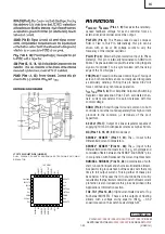
Pin 44, VID1
: One of the six logic VID pins to program the output
voltage.
Pin 45, VID2
: One of the six logic VID pins to program the output
voltage.
Pin 46, VID3
: One of the six logic VID pins to program the output
voltage.
Pins 47, NC
: No connect.
Pins 48, NC
: No connect.
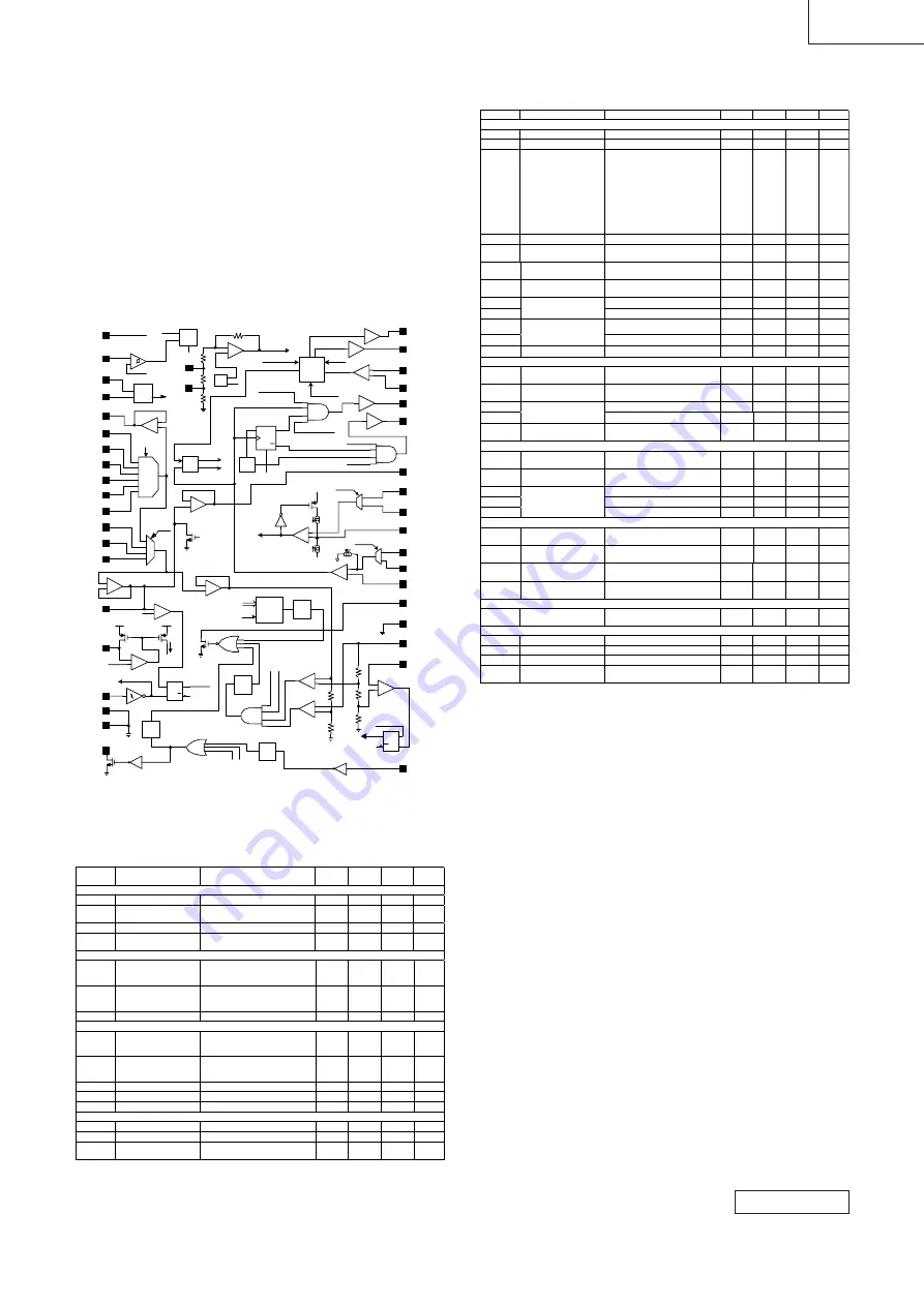
Block Diagram
+
-
POR
Mode
Logic
+
-
PSI#
SGND
VDD
DPSLP#
DPRSLP
P_Z1
P_Z0
1.255V
1.708V
DGND
VDAC
VDPSLP
+
-
VBOOT
VDPRSLP
V1R7
+
-
5V
5V
1.708V
VR_ON
+
-
+
-
+
-
soft_off
1-Phase
Logic
+
-
SYNC1
SYNC2
PGND1
SW1
async.
vid_change
OUT1
Q
Q
SET
CL R
D
drv1_enable
current_lim#
enable#
OUT2
drv2_enable
Logic
drv1_enable
drv2_enable
+
-
VREF
enable#
0.2V
+
-
mode
0.5 x ih
ILIM1
ILIM2
ILIMREF
2.5 x ih
5V
current_lim
5V
+
-
CMP1
CMP2
CMPREF
XOR
Edge
Circuit
VID0-5
mode
100
µ
s
Delay
20
µ
s
Delay
+
-
+
-
+
-
OV
VOVP
SENSE
MCH_OK
6ms
Delay
CLK_EN#
20
µ
s
Delay
ovp
enable#
s
o
ft
_
o
ff
por
PGOOD
Q
Q
R
S
enable
1.255V
uvlo
1.255V
BG
Bias
por
mode
1.708V
soft_start
s
of
t_of
f
por
Q
Q
R
S
SS
phase
phase
ih
ih
.88
.80
TGND
VID0
VID1
VID2
VID3
VID4
VID5
S>R
6-Bit
DAC
50ns
current_lim#
async.
Electrical Characteristics
Specifications with standard typeface are for T
J
= 25
o
C, and those with
boldface type
apply over a junction
temperature range of -5
o
C to +110
o
C. VDD = 5V, SGND = DGND = PGND1 = 0V, unless otherwise stated.
(Notes 4)
Symbol
Parameter
Conditions
Min
Typ
Max
Units
Chip Supply
VDD Shutdown Current
VR_ON = 0V, VDD = 6V.
1
10
µ
A
VDD Normal Operating
Current
VR_ON = 3.3V.
3.0
4.2
mA
UVLO Threshold
VDD = V5A = V5B, rising from 0V.
3.9
4.1
4.3
V
UVLO Hysteresis
VDD = V5A = V5B falling from
UVLO Threshold.
0.2
0.35
V
Logic
VR_ON, DPSLP#,
MCH_OK and DPRSLP
Input Logic High
VR_ON, DPSLP#, MCH_OK or
DPRSLP rising from 0V.
2.31
1.9
V
VR_ON, DPSLP#,
MCH_OK and DPRSLP
Input Logic Low
VR_ON, DPSLP#, MCH_OK or
DPRSLP falling from 3.3V.
1.43
0.99
V
CLK_EN# Sink Current
CLK_EN# = 0.1V and asserted.
2
3.2
mA
Power Good
Power Good Upper
Threshold As A Percent-
age of VREF
SENSE voltage rising from 0V.
108
112
116
%
Power Good Lower
Threshold As A Percent-
age of VREF
SENSE voltage falling from above
VREF.
84.5
87
90.5
%
Hysteresis
2
%
Power Good Delay
3.6
µ
s
PGOOD Sink Current
PGOOD = 0.1V and asserted.
2
3
mA
Output Voltage Slew Rate Control
Soft Start Current
SS = 0V.
16
22
32
µ
A
Soft Shutdown Current
33
45
57
µ
A
SpeedStep
¥
and Mode
Change Slew Rate Con-
255
335
415
µ
A
trol Current
DAC and References
VID Pins Input Logic High
0.63
V
VID Pins Input Logic Low
0.315
V
DAC Accuracy
Measured at VREF pin.
-5
°
C < Tj < 85
°
C
DAC codes from 0.844V to 1.708V.
DAC codes from 0.700V to 0.828V.
-5
°
C < Tj < 110
°
C
DAC codes from 0.844V to 1.708V.
DAC codes from 0.700V to 0.828V.
-1.0
-1.3
-1.3
-1.5
+1.0
+1.3
+1.3
+1.5
%
V1R7 Accuracy
17k
Ω
from V1R7 to GND.
-1.674
1.708
+1.742
V
VDPSLP Offset
VDPSLP = 1.398V, Measured at
VREF pin.
-4.5
+4.5
mV
VBOOT Offset
VBOOT = 1.00V, Measured at
VREF pin.
-4.5
+4.5
mV
VDPRSLP Offset
VDPRSLP = 0.748V, Measured at
VREF pin.
-4.5
+4.5
mV
source
1.5
mA
VREF Driving Capability
sink
11.7
mA
source
1.4
mA
VDAC Driving Capability
sink
14.3
mA
V1R7 Driving Capability
source
580
µ
A
Error Comparator
Error Comparator Input
Bias Current (Sourcing)
CMP1 = CMP2 = 1.436V.
12
21
38
µ
A
Error Comparator Input
Offset Voltage
CMPREF = 1.436V.
-2
+2
mV
R
hys
= 17k
Ω
82
98
115
µ
A
Hysteresis Current
R
hys
= 170k
Ω
10
µ
A
Error Comparator Propa-
gation Delay
20mV overdrive
70
ns
Current Limit
Current Limit Comparator
Input Bias Current
9
21
35
µ
A
Current Limit Comparator
Input Offset Voltage
ILIMREF = 1.436V.
-2
+2
mV
R
hys
= 17k
Ω
, ILIMREF < ILIMx
255
294
345
µ
A
R
hys
= 17k
Ω
, ILIMREF > ILIMx
250
µ
A
Current Limit Setting Cur-
rent
R
hys
= 170k
Ω
, ILIMREF < ILIMx
30
µ
A
Time Delays
t
BOOT
VBOOT Voltage Holdup
Time
From assertion of MCH_OK to as-
sertion of CLK_EN#.
10
18
30
µ
s
t
CPU_PWRGD
Power Good Mask For
Initial VID Voltage Settling
From assertion of CLK_EN# to as-
sertion of PGOOD.
3
5
9
ms
Power Good Mask For
SpeedStep
¥
Change
100
133
179
µ
s
Power Good De-assertion
Delay Upon Shutdown
Delay From VR_ON de-assertion to
PGOOD de-assertion
90
ns
Over-voltage Protection
SENSE Voltage As A
Percentage of VOVP
VOVP = VREF
109
123
139
%
System
PSI# Input Logic High
0.63
V
PSI# Input Logic Low
0.315
V
PSI# Pin Leakage Current PSI# = 7.5V
100
µ
A
Soft Shutdown Finish
Threshold
0.3
V
Note 1
: Absolute maximum ratings indicate limits beyond which damage to the device may occur. Operating Ratings are
conditions under which operation of the device is guaranteed. For guaranteed performance limits and associated test
conditions, see the Electrical Characteristics table. Functional temperature range is the range within which the device
performs its intended functions, but not necessarily meeting the limits specified in the Electrical Characteristic table.
Note 2:
The maximum allowable power dissipation is calculated by using P
Dmax
= (T
Jmax
- T
A
)/
θ
JA
, where T
Jmax
is the
maximum junction temperature, T
A
is the ambient temperature, and
θ
JA
is the junction-to-ambient thermal resistance of
the specified package. The 1.56W rating results from using 150
°
C, 25
°
C, and 80
°
C/W for T
Jmax
, T
A
, and
θ
JA
respectively.
A
θ
JA
of 90
°
C/W represents the worst-case condition of no heat sinking of the 48-pin TSSOP. Heat sinking allows the
safe dissipation of more power. The Absolute Maximum power dissipation should be derated by 12.5mW per
°
C above
25
°
C ambient. The LM2729 actively limits its junction temperature to about 150
°
C.
Note 3:
For detailed information on soldering plastic small-outline packages, refer to the
Packaging Databook
available
from National Semiconductor Corporation.
Note 4:
All limits are guaranteed. All electrical characteristics having room-temperature limits are tested during produc-
tion with T
A
= T
J
= 25
°
C. All hot and cold limits are guaranteed by correlating the electrical characteristics to process and
temperature variations and applying statistical process control.


