1-28
IC
VGN-
S36C/S36GP/S36LP/S36SP/S36TP/S38CP/
S52B/
S62PS/S62PSY/S62S/
S350F/S350FP/
S360/S360P/
S370F
(J/AM
/AO
)
Confidential
MAXTG069 (MAXIM)
HIGHSPEED STEP DDOWN REGULATOR
ELECTRICAL CHARACTERISTICS
(V+ = 15V, VCC = VDD =
SHDN
= 5V,
SKIP
= GND, TA = 0°C to +85°C, unless otherwise noted. Typical values are at TA = +25 °C.)
PARAMETER
SYMBOL
CONDITIONS
MIN
TYP
MAX
UNITS
PWM CONTROLLER
VIN
Battery voltage, V+
2
28
Input Voltage Range
VBIAS
VCC, VDD
4.5
5.5
V
FB = GND
2.475
2.5
2.525
Output Voltage Accuracy
(MAX1992 Fixed)
VOUT
MAX1992
V+ = 4.5V to 28V,
SKIP
= VCC
(Note 2)
FB = VCC
1.782
1.8
1.818
V
Feedback Voltage Accuracy
(MAX1992 Adjustable)
VFB
MAX1992 V+ = 4.5V to 28V,
SKIP
= VCC
(Note 2)
0.693
0.7
0.707
V
REFIN = 0.35
×
REF
0.693
0.7
0.707
Feedback Voltage Accuracy
(MAX1993)
VFB
MAX1993
V+ = 4.5V to 28V,
SKIP
= VCC
(Note 2)
REFIN = REF
1.980
2
2.020
V
Load Regulation Error
ILOAD = 0 to 3A,
SKIP
= VCC
0.1
%
Line Regulation Error
VCC = 4.5V to 5.5V, V+ = 4.5V to 28V
0.25
%
FB Input Bias Current
IFB
-0.1
+0.1
µA
Output Adjust Range
0.7
5.5
V
FB = GND
90
190
350
MAX1992
FB = VCC or adjustable
70
145
270
OUT Input Resistance
ROUT
MAX1993
400
800
1400
k
Ω
OUT Discharge Mode
On-Resistance
RDISCHARGE
10
25
Ω
OUT Synchronous Rectifier
Discharge Mode Turn-On Level
0.2
0.3
0.4
V
Soft-Start Ramp Time
tSS
Rising edge on
SHDN
to full current limit
1.7
ms
ELECTRICAL CHARACTERISTICS (continued)
(V+ = 15V, VCC = VDD =
SHDN
= 5V,
SKIP
= GND, TA = 0°C to +85°C, unless otherwise noted. Typical values are at TA = +25 °C.)
PARAMETER
SYMBOL
CONDITIONS
MIN
TYP
MAX
UNITS
TON = GND (600kHz)
170
194
219
TON = REF (450kHz)
213
243
273
TON = open (300kHz)
316
352
389
On-Time
tON
V+ = 15V,
VOUT = 1.5V
(Note 3)
TON = VCC (200kHz)
461
516
571
ns
Minimum Off-Time
tOFF(MIN)
(Note 3)
400
500
ns
FB forced above the regulation point,
LSAT = GND
0.55
0.85
Quiescent Supply Current (VCC)
ICC
FB forced above the regulation point,
VLSAT > 0.5V
1
mA
Quiescent Supply Current (VDD)
IDD
FB forced above the regulation point
<1
5
µA
Quiescent Supply Current (V+)
I V+
25
40
µA
Shutdown Supply Current (VCC)
SHDN
= GND
<1
7
µA
Shutdown Supply Current (VDD)
SHDN
= GND
<1
5
µA
Shutdown Supply Current (V+)
SHDN
= GND, V+ = 28V,
VCC = VDD = 0 or 5V
<1
5
µA
REFERENCE
TA = +25 °C to +85°C
1.986
2
2.014
Reference Voltage
VREF
VCC = 4.5V to 5.5V,
IREF = 0
TA = 0°C to +85°C
1.983
2
2.017
V
Reference Load Regulation
∆
VREF
IREF = -10µA to 50µA
-0.01
+0.01
V
REF Lockout Voltage
VREF(UVLO) Rising edge, hysteresis = 350mV
1.95
V
REFIN Voltage Range
0.7
VREF
V
REFIN Input Bias Current
IREFIN
0.01
0.05
µA
FAULT DETECTION
Overvoltage Trip Threshold
With respect to error comparator threshold,
OVP/UVP = VCC
12
16
20
%
Overvoltage Fault Propagation
Delay
tOVP
FB forced 2% above trip threshold
10
µs
Output Undervoltage Protection
Trip Threshold
With respect to error comparator threshold,
OVP/UVP = VCC
65
70
75
%
Output Undervoltage Protection
Blanking Time
tBLANK
From rising edge of
SHDN
10
35
ms
Output Undervoltage Fault
Propagation Delay
tUVP
10
µs
PGOOD Lower Trip Threshold
With respect to error comparator threshold,
hysteresis = 1%
-13
-10
-7
%
PGOOD Upper Trip Threshold
With respect to error comparator threshold,
hysteresis = 1%
+7
+10
+13
%
PGOOD Propagation Delay
tPGOOD
FB forced 2% beyond PGOOD trip
threshold
10
µs
ELECTRICAL CHARACTERISTICS (continued)
(V+ = 15V, VCC = VDD =
SHDN
= 5V,
SKIP
= GND, TA = 0°C to +85°C, unless otherwise noted. Typical values are at TA = +25 °C.)
PARAMETER
SYMBOL
CONDITIONS
MIN
TYP
MAX
UNITS
PGOOD Output Low Voltage
ISINK = 4mA
0.3
V
PGOOD Leakage Current
IPGOOD
FB = REF (PGOOD high impedance),
PGOOD forced to 5.5V
1
µA
FBLANK = VCC
120
218
320
FBLANK = open
80
140
205
Fault Blanking Time
tFBLANK
FBLANK = REF
35
63
95
µs
Thermal Shutdown Threshold
TSHDN
Hysteresis = 15°C
160
°C
VCC Undervoltage Lockout
Threshold
VUVLO(VCC)
Rising edge, PWM disabled below this level
hysteresis = 20mV
4.1
4.25
4.4
V
CURRENT LIMIT
ILIM Adjustment Range
0.25
2.00
V
CSP
0
2.7
Current-Limit Input Range
CSN
-0.3
+28.0
V
CSP/CSN Input Current
-0.5
+0.5
µA
Valley Current-Limit Threshold
(Fixed)
VLIM(VAL)
VCSP - VCSN, ILIM = VCC
45
50
55
mV
VILIM = 250mV
15
25
35
Valley Current-Limit Threshold
(Adjustable)
VLIM(VAL)
VCSP - VCSN
VILIM = 2.00V
170
200
230
mV
Current-Limit Threshold
(Negative)
VNEG
VCSP - VCSN,
SKIP
= ILIM = VCC,
TA = +25 °C
-75
-60
-45
mV
Current-Limit Threshold
(Zero Crossing)
VZX
With respect to valley current-limit
threshold, VCSP - VCSN,
SKIP
= GND,
ILIM = VCC
2.5
mV
LSAT = VCC
180
200
220
LSAT = open
157
175
193
Inductor Saturation Current-Limit
Threshold
With respect to
valley current-limit
threshold,
ILIM = VCC
LSAT = REF
135
150
165
%
ILIM Saturation Fault Sink Current
IILIM(LSAT)
VCSP - VCSN > inductor saturation current
limit, 0.25V < VILIM < 2.0V
4
6
8
µA
ILIM Leakage Current
VCSP - VCSN < inductor saturation current
limit
0.1
µA
GATE DRIVERS
DH Gate Driver On-Resistance
RDH
BST - LX forced to 5V
1.5
5
Ω
DL, high state
1.5
5
DL Gate Driver On-Resistance
RDL
DL, low state
0.6
3
Ω
DH Gate Driver Source/Sink
Current
IDH
DH forced to 2.5V, BST - LX forced to 5V
1
A
DL Gate Driver Source Current
IDL(SOURCE) DL forced to 2.5V
1
A
ELECTRICAL CHARACTERISTICS (continued)
(V+ = 15V, VCC = VDD =
SHDN
= 5V,
SKIP
= GND, TA = 0°C to +85°C, unless otherwise noted. Typical values are at TA = +25 °C.)
PARAMETER
SYMBOL
CONDITIONS
MIN
TYP
MAX
UNITS
DL Gate Driver Sink Current
IDL(SINK)
DL forced to 2.5V
3
A
DL rising
35
Dead Time
tDEAD
DH rising
26
ns
INPUTS AND OUTPUTS
OD On-Resistance
ROD
GATE = VCC
10
25
Ω
OD Leakage Current
GATE = GND, OD forced to 5.5V
1
200
nA
Logic Input Threshold
SHDN
,
SKIP
, GATE
rising edge, hysteresis = 225mV
1.20
1.7
2.20
V
Logic Input Current
SHDN
,
SKIP
, GATE
-1
+1
µA
High
1.9
2.0
2.1
Dual Mode™ Threshold Voltage
MAX1992 FB
Low
0.05
0.1
0.15
V
High
VCC -
0.4V
Open
3.15
3.85
REF
1.65
2.35
Four-Level Input Logic Levels
TON, OVP/UVP,
LSAT, FBLANK
Low
0.5
V
Four-Level Logic Input Current
TON, OVP/UVP, LSAT,
FBLANK forced to GND or VCC
-3
+3
µA
ELECTRICAL CHARACTERISTICS
(V+ = 15V, VCC = VDD =
SHDN
= 5V,
SKIP
= GND, TA = -40°C to +85°C, unless otherwise noted.) (Note 4)
PARAMETER
SYMBOL
CONDITIONS
MIN
MAX
UNITS
PWM CONTROLLER
VIN
Battery voltage, V+
2
28
Input Voltage Range
VBIAS
VCC, VDD
4.5
5.5
V
FB = GND
2.462
2.538
Output Voltage Accuracy
(MAX1992 Fixed)
VOUT
MAX1992,
V+ = 4.5V to 28V,
SKIP
= VCC
(Note 2)
FB = VCC
1.773
1.827
V
Feedback Voltage Accuracy
(MAX1992 Adjustable)
VFB
MAX1992, V+ = 4.5V to 28V,
SKIP
= VCC
(Note 2)
0.689
0.711
V
REFIN = 0.35
×
REF
0.689
0.711
Feedback Voltage Accuracy
(MAX1993)
VFB
MAX1993,
V+ = 4.5V to 28V,
SKIP
= VCC
(Note 2)
REFIN = REF
1.970
2.030
V
TON = GND (600kHz)
170
219
TON = REF (450kHz)
213
273
TON = open (300kHz)
316
389
On-Time
tON
V+ = 15V,
VOUT = 1.5V
(Note 3)
TON = VCC (200kHz)
461
571
ns
Dual Mode is a trademark of Maxim Integrated Products, Inc.
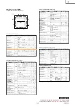
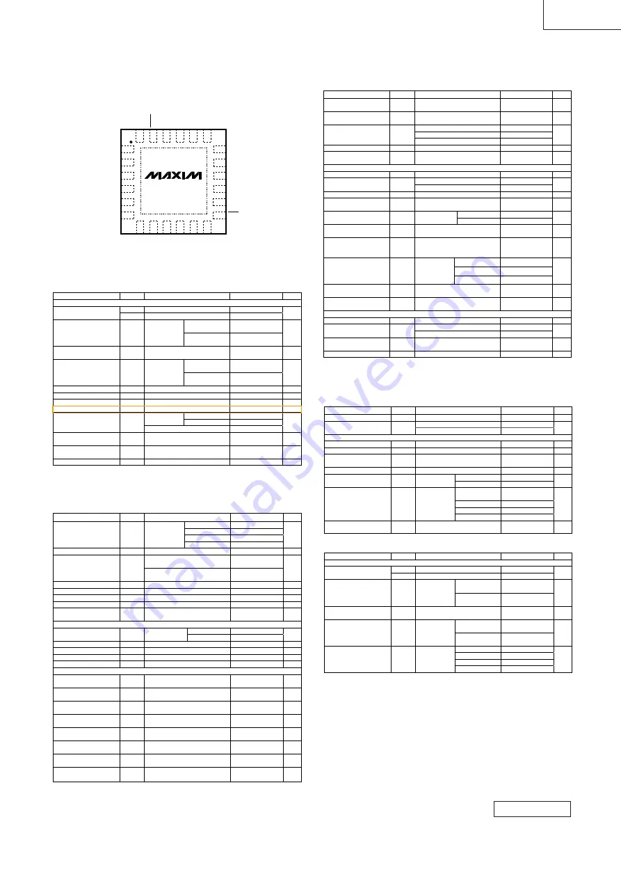
24
23
22
21
20
1
2
3
4
5
7
8
9
10
11
14
15
16
17
18
TOP VIEW
MAX1993
DL
TON
FBLANK
LSAT
PGOOD
ILIM
6
REF
BST
DH
V+
13 SKIP
LX
CSP
OUT
12
CSN
FB
OD
REFIN
OVP/UVP
SHDN
V
CC
GA
TE
GND
19
V
DD


