background image

3-10

WRR-802A (U)

3. Frequency characteristic check

Procedure

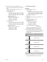
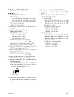
(1) Set the WRR-802A as follows;

Channel setting:

U64 model; Group 00, 6501 channel (776.125 MHz)

U66 model; Group 00, 6701 channel (788.125 MHz)
U68 model; Group 00, 6901 channel (800.125 MHz)

VOL. control: MAX
Muting: OFF

TUNER OUTPUT LEVEL switch: LINE (

_

20 dBm)

(2) Connect the audio analyzer to the TUNER OUTPUT

(XLR type) connector via MIC amp (Amplification
gain 0 dB).

(3) Connect the signal generator to the ANTENNA A IN

connector.

(4) Set the signal generator as follows:

Signal generator setting

FREQUENCY(carrier frequency)

U64 model; 776.125 MHz

U66 model; 788.125 MHz
U68 model; 800.125 MHz

RF OUTPUT (Output level): 60 dB

u

V

EMF

(= 

_

53 dBm)

MODULATION (Modulation frequency): 1 kHz
DEVIATION (Frequency deviation): 

±

12 kHz

(5) Read the output level of the TUNER OUTPUT (XLR

type) connector (indication of the audio analyzer). This

level is specified to be 0 dB.

(6) Change the MODULATION (modulation frequency)

of the signal generator as follows, and check the output
level with respect to the output level under the proce-

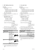
dure (5) is set also as follows.

n

100 Hz and 15 kHz modulation frequency must be set
by using the function generator.

MODULATION frequency

TUNER OUTPUT connector

of signal generator

output level

100 Hz

_

0.7 

±

1.0 dB

15 kHz

_

28.5 

±

2.5 dB

(7) Connect the audio analyzer to the TUNER OUTPUT

(TRS type) connector via the MIC amp (Amplification

gain 0 dB).

(8) Perform the procedures (5) and (6).

(9) Connect the signal generator to the ANTENNA B IN

connector, and perform the procedures (4) through (8).

4. Distortion ratio check

Procedure

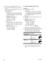
(1) Set the WRR-802A as follows;

Channel setting:

U64 model; Group 00, 6501 channel (776.125 MHz)

U66 model; Group 00, 6701 channel (788.125 MHz)
U68 model; Group 00, 6901 channel (800.125 MHz)

VOL. control: MAX
Muting: OFF

TUNER OUTPUT LEVEL switch: LINE (

_

20 dBm)

(2) Connect the audio analyzer to the TUNER OUTPUT

(XLR type) connector via MIC amp (Amplification
gain 0 dB).

(3) Connect the signal generator to the ANTENNA A IN

connector.

(4) Set the signal generator as follows:

Signal generator setting

FREQUENCY(carrier frequency)

U64 model; 776.125 MHz

U66 model; 788.125 MHz
U68 model; 800.125 MHz

RF OUTPUT (Output level): 60d B

u

V

EMF

(= 

_

53 dBm)

MODULATION (Modulation frequency): 1 kHz
DEVIATION (Frequency deviation): 

±

40 kHz

(5) Set the audio analyzer to the distortion mode, and

check that the distortion ratio is less than 0.7 %.

(6) Change the MODULATION (modulation frequency)

of the signal generator as shown below.

MODULATION (modulation frequency): 10 kHz
(Note: 10 kHz modulation frequency must be set by

using the function generator.)
Check that the distortion ratio is less than 4 %.

(7) Connect the audio analyzer to the TUNER OUTPUT

(TRS type) connector via the MIC amp (Amplification

gain 0 dB).

(8) Perform the procedures (5) and (6).

(9) Connect the signal generator to the ANTENNA B IN

connector, and perform the procedures (5) through (8)

above.

Summary of Contents for WRR-802A

Page 1: ...UHF SYNTHESIZED DIVERSITY TUNER WRR 802A SERVICE MANUAL U Model 1st Edition Printed in Japan Sony Corporation 1999 6 11 Broadcasting Professional Systems Company 1999 WRR 802A U E 9 976 876 01 ...

Page 2: ...e Gefahr eines elektrischen Schlages Feuergefahr und Verletzungen zu vermeiden sind bei Wartungsarbeiten strikt die Angaben in der Anleitung zu befolgen Andere als die angegeben Wartungsarbeiten dürfen nur von Personen ausgeführt werden die eine spezielle Befähigung dazu besitzen AVERTISSEMENT Ce manual est destiné uniquement aux personnes compétentes en charge de l entretien Afin de réduire les r...

Page 3: ... 3 3 Electrical Alignment 3 1 Preparation 3 1 3 1 1 Equipment and Tools 3 1 3 2 Adjustment 3 2 3 2 1 Tuner Unit Adjustment 3 3 3 2 2 Overall Characteristics Check 3 8 4 Semiconductor Pin Assignments 5 Spare Parts 5 1 Notes on Repair Parts 5 1 5 2 Exploded Views 5 2 5 3 Electrical Parts List 5 4 5 4 Accessories Supplied 5 12 6 Block Diagrams Overall Block Diagram 6 2 Tuner Unit Block Diagram 6 3 7 ...

Page 4: ...R 261 Board 7 2 DP 305 Board Tuner unit 7 3 RF 92 Board Tuner unit 7 3 8 Schematic Diagrams CN 1922 Board 8 1 CN 1923 Board 8 2 MB 872 Board 8 2 RE 176 Board 8 2 VR 261 Board 8 2 DP 305 Board Tuner unit 8 6 RF 92 Board Tuner unit 8 4 ...

Page 5: ...s may damage the finish of the case Never install the unit on or near a heat source such as lighting equipment or power amplifiers Avoid using in very humid or dusty places because such use may shorten the life of the unit To avoid degradation of the signal to noise ratio do not use the unit in noisy places or in locations subject to vibration such as the following near electrical equipment such a...

Page 6: ...lights and the indications appear when the audio output level is higher than the reference level 3 BATT battery indicator 4 BATT battery indication Indicate the condition of the wireless microphone transmitter batteries The indicator and indication appear and start flashing about one hour before the transmitter batteries go flat The time at which flashing begins will depend on the type of battery ...

Page 7: ...lied antennas and make the antenna tips point upward 2 Connect the supplied AC power adaptor to the DC IN 9V connector and an audio mixer or amplifier to the TUNER OUTPUT connector ANTENNA A B Audio mixer amplifier AC power adaptor UHF synthesized transmitter UHF synthesized wireless microphone DC IN 9V TUNER OUTPUT 5 3 4 1 2 Operation 3 Turn the POWER switch on Note Turn the POWER switch on after...

Page 8: ...luded for compliance with frequency regulations in various countries and will not always guarantee interference free operation Group 00 is used to scan for open channels or to use only for a one channel system Directrices para el uso de sistemas multicanal Este producto se ha diseñado para proporcionar una operación excelente sin interferencias en sistemas de múltiples canales Para esto Sony recom...

Page 9: ...5 805 625 Frequency MHz Frequencia Fréquence L 5 Group L1 7 channel group Use when TV channel 68 is open Grupo L1 Grupo de 7 canales Se utiliza cuando el canal de TV 68 está abierto Groupe L1 Groupe de 7 canaux Lorsque le canal de télévision 68 est ouvert Group L2 7 channel group Use when TV channel 68 is open Grupo L2 Grupo de 7 canales Se utiliza cuando el canal de TV 68 está abierto Groupe L2 G...

Page 10: ...oup Use when TV channel 66 is open Grupo L1 Grupo de 7 canales Se utiliza cuando el canal de TV 66 está abierto Groupe L1 Groupe de 7 canaux Lorsque le canal de télévision 66 est ouvert Group L2 7 channel group Use when TV channel 66 is open Grupo L2 Grupo de 7 canales Se utiliza cuando el canal de TV 66 está abierto Groupe L2 Groupe de 7 canaux Lorsque le canal de télévision 66 est ouvert Group H...

Page 11: ...o A2 para modelos de las versiones 66 y 68 pueden utilizarse de forma combinada Consulte Grupo A2 en las páginas 4 y 8 Groupe A2 groupe de 13 canaux Pour utiliser simultanément jusqu à 13 canaux sélectionnés dans la bande de fréquence des canaux de télévision impairs sur ceux captables par les trois versions du syntoniseur Les canaux signalés comme formant le Groupe A2 pour les modèles 66 et 68 pe...

Page 12: ......

Page 13: ...t Check the tuner unit then fix a faulty section and perform 3 Electrical Alignment NO TONE As no tone signal is available or a Make sure that the transmitter is turned on If it is then the problem lies in the tone signal other than 32 768 kHz transmitter s tone signal generator or the tuner s tone squelch circuit is being received the audio signal If you are using a WRT 810A wireless microphone a...

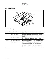
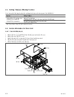
Page 14: ...releasing Normal operation mode Turn OFF the POWER switch Default Factory Setting Muting OFF mode is released Normal mode 2 4 Service Information for Tuner Unit 2 4 1 Tuner Unit Removal 1 Remove the four screws BTT M3 from the side panel and remove the cover 2 Remove the screw BVTT2 6 x 5 3 Remove the gasket T1 and gasket T2 from the rail and the tuner unit 4 Desolder the connection plate from the...

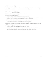
Page 15: ...l components other than the tuner unit such as MB 872 board CN 1922 board CN 1923 board harness etc then fix a faulty section If there is a fault tuner unit is defective Check the tuner unit then fix a faulty section and perform 3 Electrical Alignment 3 In order to prove the whole WRR 802A change the tuner unit of the repairing WRR 802A with WRU 806A quality unit 4 Check the fault of repairing WRR...

Page 16: ......

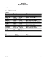
Page 17: ...3B equivalent RF millivolt meter Frequency 10 kHz to 1000 MHz MEGURO MV 19B C with 50 Z termination prove chip MP 3109 or equivalent Level meter Frequency 20 Hz to 100 kHz Noise meter Frequency 10 Hz to 500 kHz MEGURO MN 445B or equivalent Filter included A weighted filter Tracking generator Frequency 100 kHz to 2 GHz ADVANTEST TR4153A or equivalent Function generator 32 768 kHz and 32 782 kHz 1 H...

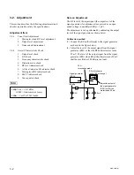
Page 18: ...e on Adjustment The RF level of the input signal the output level of the signal generator for adjustment is expressed as an open ended voltage in unit dBu 0 dBu 1 uV The adjustment is to be performed by calibrating the output level of the signal generator as shown below Calibration method 1 Connect the RF millivoltmeter to the signal generator as shown in the figure below 2 Adjust the level of the...

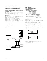
Page 19: ...nnection Procedure Step 1 Preparation Set the signal generator as follows Signal generator setting FREQUENCY carrier frequency U64 model 772 000 MHz U66 model 784 000 MHz U68 model 796 000 MHz RF OUTPUT Output level 35 dBuVEMF _78 dBm MODULATION Modulation frequency OFF No modulation Step 2 Adjustment 1 Connect the signal generator to the ANTENNA A IN connector 2 Turn OFF the WRR 802A POWER switch...

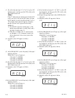
Page 20: ...ner unit 11 Indication on the LCD appears as follows LCD 12 Set the FREQUENCY carrier frequency of the signal generator as follow FREQUENCY carrier frequency U64 model 780 000 MHz U66 model 792 000 MHz U68 model 804 000 MHz A C2 L A C2 L A C3 L A C3 L 13 Check first that indication L of AC3L on the LCD has disappeared and then press the S708 switch on the RF 92 board tuner unit 14 Connect the sign...

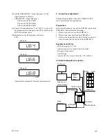
Page 21: ... the TUNER OUTPUT levels deviate from the specification Preparation Before the adjustments turn off the POWER switch of the WRR 802A and perform the followings 1 Remove the case cover of the WRR 802A 2 Remove the tuner unit from the WRR 802A 3 Remove the upper side case lid of the tuner unit and insert the tuner unit to the slot of the WRR 802A Equipment and Tools DC power supply 9 Vdc Audio analy...

Page 22: ...e and the ANTENNA should be within 0 3 dB Step 3 After completing adjustment turn off the WRR 802A power switch and perform the followings 1 Remove the tuner unit from the WRR 802A 2 Attach the upper side case lid to the tuner unit and insert the tuner unit to the slot of the WRR 802A 3 Noise squelch adjustment Equipment and Tools DC power supply 9 Vdc Signal generator Audio analyzer level meter d...

Page 23: ...eviation 5 kHz 4 Adjust the RF OUTPUT Output level of the signal generator so that Signal to Noise ratio is 34 dB 5 dB S N 34 dB 5 dB under the Step 1 S N check 5 Turn 1RV205 tuner unit slowly counterclockwise to be the DC voltage of the TP201 NOISE terminal land change L about 0 V 6 Adjustment Specification DC voltage of the TP201 NOISE terminal land change from L about 0 V to H about 4 8 V level...

Page 24: ...3 dBm MODULATION Modulation frequency 1 kHz DEVIATION Frequency deviation 5 kHz 5 Check that the TUNER OUTPUT XLR type connec tor output level is _21 dBm 1 5 dB at 600 Z loaded 6 Connect the audio analyzer to the TUNER OUTPUT TRS type connector via the MIC amp Amplification gain 0 dB 7 Check that the TUNER OUTPUT TRS type connec tor output level is _21 dBm 1 5 dB at 600 Z loaded 8 Connect the sign...

Page 25: ...l 20 dBuVEMF _93 dBm 9 Check that output level of the TUNER OUTPUT XLR type is _50 dB or less S N is 50 dB or more with A weighted filter as compared with the level of procedure 5 above 10 Change the RF OUTPUT output level of the signal generator as shown below RF OUTPUT output level 60 dBuVEMF _53 dBm 11 Set the audio analyzer to the distortion mode 12 Check that distortion ratio is _45 dB or les...

Page 26: ...UT TRS type connector via the MIC amp Amplification gain 0 dB 8 Perform the procedures 5 and 6 9 Connect the signal generator to the ANTENNA B IN connector and perform the procedures 4 through 8 4 Distortion ratio check Procedure 1 Set the WRR 802A as follows Channel setting U64 model Group 00 6501 channel 776 125 MHz U66 model Group 00 6701 channel 788 125 MHz U68 model Group 00 6901 channel 800 ...

Page 27: ...02A as follows Channel setting U64 model Group 00 6501 channel 776 125 MHz U66 model Group 00 6701 channel 788 125 MHz U68 model Group 00 6901 channel 800 125 MHz VOL Control Any position Muting ON 2 Connect the signal generator to the ANTENNA A IN connector 3 Set the signal generator as follows Signal generator setting FREQUENCY carrier frequency U64 model 776 125 MHz U66 model 788 125 MHz U68 mo...

Page 28: ...802A as follows Channel setting U64 model Group 00 6501 channel 776 125 MHz U66 model Group 00 6701 channel 788 125 MHz U68 model Group 00 6901 channel 800 125 MHz VOL control Any position Muting OFF 2 Connect the signal generator to the ANTENNA A IN connector 3 Set the signal generator as follows Signal generator setting FREQUENCY carrier frequency U64 model 776 125 MHz U66 model 788 125 MHz U68 ...

Page 29: ...NE message disappears on LCD 7 Increase gradually the RF OUTPUT output level of the signal generator Check that RF OUTPUT output level is 25 dBuVEMF 5 dB at when RF Indicator lights green LED and NO TONE message appears on LCD 8 Connect the signal generator to the ANTENNA B IN connector and perform the procedures 3 through 7 above 9 Set the channel setting and FREQUENCY carrier frequency of the si...

Page 30: ...seconds OFF BATT indicator LCD Goes out BATT indicator LED Goes out 5 Connect the signal generator to the ANTENNA B IN connector and perform the procedures 3 and 4 above AF BATT AF BATT 9 Tone squelch check Procedure 1 Set the WRR 802A as follows Channel setting U64 model Group 00 6501 channel 776 125 MHz U66 model Group 00 6701 channel 788 125 MHz U68 model Group 00 6901 channel 800 125 MHz VOL c...

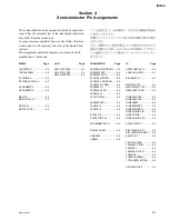
Page 31: ... T 4 5 TA31161FN EL 4 5 TA78L05F TE12L 4 4 TA8122AF 4 5 TA8122AF J TP2 4 5 TC4S69F 4 6 TC4S69F TE85R 4 6 TC74HC4053AFT EL 4 6 UPC4574G2 E2 4 6 2SA1832 YGR TE85L1 4 2 2SB1202FAST 4 2 2SB1202FAT TL 4 2 2SC4726LN TLPQ 4 2 2SC4738 YGR TE85L 4 2 2SC4915 O TE85L 4 2 2SD1048 X7 4 2 2SD1048X6 TB 4 2 2SD2216 Q 4 2 2SJ377 TE16L 4 2 3SK239AXRTL 4 2 3SK254 T2 4 2 3SK255 T2 4 2 DTC323TK 4 2 DTC323TKT146 4 2 MT...

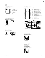
Page 32: ...TB TOP VIEW SML 310DTT86 SML 310LTT86 SML 310MTT86 TOP VIEW 2SA1832 YGR TE85L1 2SB1202FAST 2SB1202FAT TL TOP VIEW 2SC4726LN TLPQ 2SC4738 YGR TE85L 2SC4915 O TE85L 2SD1048 X7 2SD1048X6 TB 2SD2216 Q TOSHIBA S 2SJ377 TE16L G2 G1 WIDE 3SK239AXRTL S D G2 G1 WIDE 3SK254 T2 3SK255 T2 R1 TOP VIEW DTC323TK R1 2 2 k DTC323TKT146 S MTD20N06HDLT4 1 2 3 6 5 4 TOP VIEW 1 5 6 2 3 4 UMX2NTL R1 R2 TOP VIEW RN1104 ...

Page 33: ...00 kHz 100 kHz ANALOG SUPPLY VOLTAGE INPUT 5 V INVERTING COMPENSATION CAPACITOR STEP UP COMPENSATION CAPACITOR CURRENT SENSE HIGH INVERTING SECTION CURRENT SENSE HIGH STEP UP SECTION CURRENT SENSE LOW INVERTING SECTION CURRENT SENSE LOW STEP UP SECTION INVERTING SECTION FEEDBACK INPUT STEP UP FEEDBACK INPUT VOLTAGE INPUT SOFT START TIMING CAPACITOR HIGH CURRENT SUPPLY VOLTAGE INPUT 5 V PUSH PULL O...

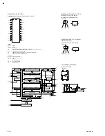
Page 34: ...SCout P0 P3 LD fp1 fp2 fr2 CLOCK DATA RF PLL1 2 CHARGE PUMP OUTPUT CURRENT ADJUSTMENT LOAD ENABLE OF SERIAL INPUT DATA H DATA IS SHIFTED INTO A LATCH CRYSTAL OSCILLATOR OR TCXO POWER SAVING MODE CONTROL L POWER SAVING MODE POWER SUPPLY FOR CHARGE PUMP CHARGE PUMP PLL1 2 CRYSTAL OSCILLATOR DATA LOCK DETECTOR fp1 fp2 MONITORING fr2 MONITORING POWER SAV POWER SAV CRYSTAL OSCILLATOR PHASE CHARGE 17 BI...

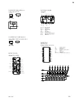
Page 35: ...MIXER OUTPUT BIAS FOR IF INPUT IF INPUT RSSI OUTPUT IF LIMITTER OUTPUT PHASE INPUT FOR FM DETECTOR DEMODULATION SIGNAL OUTPUT MIXER INPUT OSC IN OUT BS MIXER OUT DEC IF IN RSSI IF OUT1 2 QUAD AF OUT MIX IN 16 VCC2 IF DETECTOR TOP VIEW S 80735SN DZ T1 SEIKO INSTR 3 5 V S 81250SGUP DQD T1 SEIKO I E 5 0 V SA575DK T PHILIPS TA31161FN EL TOSHIBA TA8122AF TSB TA8122AF J TP2 1 SIN 2 CK 3 LATCH 4 SOUT 5 E...

Page 36: ... 5 6 7 8 16 15 14 13 12 11 10 9 Y I O X I O X1 I O X0 I O A IN B IN C IN GND VDD VEE OPEN A 11 OPEN B 10 OPEN C 9 A 0 1 0 1 0 1 0 1 x SELECT EN ON CHANNEL Z0 Z0 Z0 Z0 Z1 Z1 Z1 Z1 Y0 Y0 Y1 Y1 Y0 Y0 Y1 Y1 X0 X1 X0 X1 X0 X1 X0 X1 OPEN 0 1 x LOW LEVEL HIGH LEVEL DON T CARE C MOS TRIPLE 2 CHANNEL ANALOG MULTIPLEXER DEMULTIPLEXER TOP VIEW TC4S69F TOSHIBA TC4S69F TE85R TC74HC4053AFT EL TOSHIBA UPC4574G2 ...

Page 37: ... 802 A MB 806 A COM0 COM3 38 41 LCD control SEG0 SEG19 42 61 LCD control VL 34 Bias voltage control for LCD LED RF 71 Control for RF LED H ON LED AF 76 Control for AF LED H ON LED BATT 20 Control for BATT LED H ON DIV 66 Diversity control H ANT A L ANT B AFM 67 AF muting control H Muting OFF Inputs Outputs for EEPROM and PLL Singal Name Pin No Description ROM DO 17 EEPROM control ROM CS 68 EEPROM ...

Page 38: ......

Page 39: ...used in the case of replacement 2 Standardization of Parts Some repair parts supplied by Sony differ from those used for the unit These are because of parts common ality and improvement Parts list has the present standardized repair parts 3 Stock of Parts Parts marked with o at SP Supply Code column of the spare parts list may not be stocked Therefore the delivery date will be delayed ...

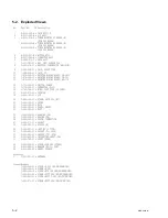
Page 40: ...94 11 s WIRE FLAT TYPE 35 CORE 17 2 536 671 01 s CUSHION 18 2 545 180 03 o LID 19 2 545 186 01 s SCREW BTP 2X5 W2 20 2 545 188 01 o COVER 21 2 545 189 02 o RAIL 22 2 545 190 11 o PANEL FRONT 23 2 545 194 01 o FOOT 24 2 545 196 01 o BARRIER SW 25 2 545 206 01 o SPACER PB 26 2 545 363 01 s PLATE CONNECTION 27 2 545 371 01 s GASKET 28 2 545 383 01 s SPACER B 29 2 545 387 11 s BTT M3 S TITE 30 2 545 4...

Page 41: ...20 29 29 21 34 13 9 11 15 4 23 33 25 23 8 22 8 37 36 BVTT 3x6 BTP 3x8 BVTT 2 6x5 BVTT 3x6 BVTT 3x6 BVTT 3x6 BVTT 3x6 29 K 3x5 K 3x5 K 3x5 24 14 12 10 26 31 30 32 7 18 28 3 18 2 1 16 27 19 17 BVTT 2 x 4 BVTT2 x 4 2 1 1 2 37 35 6 19 ...

Page 42: ...TOR CERAMIC 1000PF 50V B C2209 1 162 964 11 s CAPACITOR CERAMIC 1000PF 50V B C2210 1 162 910 11 s CAPACITOR CERAMIC 5PF 50V 1608 C2211 1 162 912 11 s CAPACITOR CERAMIC 7PF 50V 1608 C2212 1 162 964 11 s CAPACITOR CERAMIC 1000PF 50V B C2214 1 162 964 11 s CAPACITOR CERAMIC 1000PF 50V B C2301 1 163 251 11 s CAPACITOR CERAMIC 100PF 50V C2303 1 162 974 11 s CAPACITOR CERAMIC 0 01MF 50V F CN111 1 569 66...

Page 43: ...67 11 s CAPACITOR CERAMIC 3300PF 50V B C1010 1 135 177 21 s CAPACITOR TANTALUM 1MF 25V C1011 1 135 177 21 s CAPACITOR TANTALUM 1MF 25V C1012 1 115 758 11 s CAPACITOR ELECT 470MF 16V 105C C1013 1 107 826 11 s CAPACITOR CHIP CERAMIC 0 1MF C1014 1 115 758 11 s CAPACITOR ELECT 470MF 16V 105C C1015 1 115 758 11 s CAPACITOR ELECT 470MF 16V 105C C1016 1 164 156 11 s CAPACITOR CERAMIC 0 1MF 25V F C1017 1 ...

Page 44: ...01 8 729 015 39 s TRANSISTOR DTC323TK 300MW Q1102 8 729 015 39 s TRANSISTOR DTC323TK 300MW Q1103 8 729 015 39 s TRANSISTOR DTC323TK 300MW Q1104 8 729 015 39 s TRANSISTOR DTC323TK 300MW Q1201 8 729 425 64 s TRANSISTOR 2SD2216Q Q1202 8 729 425 64 s TRANSISTOR 2SD2216Q Q1203 8 729 425 64 s TRANSISTOR 2SD2216Q Q1301 8 729 015 39 s TRANSISTOR DTC323TK 300MW Q1302 8 729 015 39 s TRANSISTOR DTC323TK 300M...

Page 45: ...1 s CAPACITOR CERAMIC 7PF 50V 1608 C118 1 162 970 11 s CAPACITOR CERAMIC 0 01MF 25V B C120 1 162 970 11 s CAPACITOR CERAMIC 0 01MF 25V B C123 1 162 970 11 s CAPACITOR CERAMIC 0 01MF 25V B C124 1 162 926 11 s CAPACITOR CERAMIC 82PF 50V CH C125 1 162 970 11 s CAPACITOR CERAMIC 0 01MF 25V B C126 1 164 227 11 s CAPACITOR CERAMIC 0 022MF 25V C128 1 107 826 11 s CAPACITOR CHIP CERAMIC 0 1MF C129 1 107 8...

Page 46: ... C270 1 162 970 11 s CAPACITOR CERAMIC 0 01MF 25V B C291 1 104 851 11 s CAPACITOR TANTALUM 10MF 10V C292 1 104 851 11 s CAPACITOR TANTALUM 10MF 10V C302 1 162 907 11 s CAPACITOR CERAMIC 2PF 50V CK TUNER RF 92 BOARD Ref No or Q ty Part No SP Description C303 1 162 964 11 s CAPACITOR CERAMIC 1000PF 50V B C304 1 162 964 11 s CAPACITOR CERAMIC 1000PF 50V B C305 1 162 964 11 s CAPACITOR CERAMIC 1000PF ...

Page 47: ...ACITOR CERAMIC 0 01MF 25V B C706 1 162 970 11 s CAPACITOR CERAMIC 0 01MF 25V B C709 1 162 970 11 s CAPACITOR CERAMIC 0 01MF 25V B C710 1 162 970 11 s CAPACITOR CERAMIC 0 01MF 25V B C722 1 104 851 11 s CAPACITOR TANTALUM 10MF 10V C740 1 107 826 11 s CAPACITOR CHIP CERAMIC 0 1MF C741 1 104 851 11 s CAPACITOR TANTALUM 10MF 10V C742 1 162 970 11 s CAPACITOR CERAMIC 0 01MF 25V B C753 1 162 907 11 s CAP...

Page 48: ...01 1 412 955 11 s INDUCTOR 22UH 2520 Q101 8 729 035 13 s TRANSISTOR 3SK239AXRTL Q102 8 729 047 26 s TRANSISTOR 3SK255 T2 Q103 8 729 047 26 s TRANSISTOR 3SK255 T2 Q104 8 729 047 25 s TRANSISTOR 3SK254 T2 Q105 8 729 047 25 s TRANSISTOR 3SK254 T2 Q201 8 729 800 37 s TRANSISTOR 2SD1048X7 Q203 8 729 429 18 s TRANSISTOR UN9213 Q302 8 729 033 87 s TRANSISTOR 2SC4726LN TLPQ Q303 8 729 033 87 s TRANSISTOR ...

Page 49: ... 2K 1 16W 1608 R275 1 216 854 11 s RESISTOR CHIP 560K 1 16W R276 1 216 833 11 s RESISTOR CHIP 10K 1 16W 1608 TUNER RF 92 BOARD Ref No or Q ty Part No SP Description R277 1 216 845 11 s RESISTOR CHIP 100K 1 16W 1608 R278 1 216 821 11 s RESISTOR CHIP 1 0K 1 16W 1608 R279 1 216 843 11 s RESISTOR CHIP 68K 1 16W 1608 R280 1 216 845 11 s RESISTOR CHIP 100K 1 16W 1608 R281 1 216 825 11 s RESISTOR CHIP 2 ...

Page 50: ...762 1 216 837 11 s RESISTOR CHIP 22K 1 16W 1608 R763 1 216 837 11 s RESISTOR CHIP 22K 1 16W 1608 R764 1 216 837 11 s RESISTOR CHIP 22K 1 16W 1608 R765 1 216 837 11 s RESISTOR CHIP 22K 1 16W 1608 R766 1 216 837 11 s RESISTOR CHIP 22K 1 16W 1608 R767 1 216 837 11 s RESISTOR CHIP 22K 1 16W 1608 R770 1 216 837 11 s RESISTOR CHIP 22K 1 16W 1608 R790 1 216 821 11 s RESISTOR CHIP 1 0K 1 16W 1608 R791 1 2...

Page 51: ...d by the AF amplifier A and AF amplifier B and is sent to the diversity switching cir cuit The diversity switching is controlled by the DIV signal from the CPU The audio output signal from the diversity switching circuit is passed through the muting circuit de em phasis circuit low pass filter circuit and expander circuit then amplified by the AF amplifier Section 6 Block Diagrams DP 305 board The...

Page 52: ... DC CONVERTER POWER SWITCH 15V 9V 9V DC 9V IN REG 12V REG RF Block 12V VR 261 board RE 176 board CN1101 CN1003 CN1103 CN1102 J1101 J1001 J1701 J1702 15 V 9 V REGULATOR CN1004 IC1006 IC1101 IC1001 IC1004 IC1005 IC1101 CN1201 RV1201 L1006 Q2101 Q2201 MUTE IC1303 IC1302 IC1103 IC1102 CN 1923 board S1801 RF Block AF Block ...

Page 53: ...SAWF 2nd Mixer IF Amp Discriminator Ant IN B R F Block A Buffer B 2nd LO Diversity Mute De emphasis Expander AF Amp AF OUT AF Det Noise Det Tone Det AF Amp A AF Amp B PLL VCO IC601 Buffer A Switch AF B AF A CPU 140 05MHz 150 75MHz 150 75MHz 10 7MHz 10 7MHz fr 150 75MHz 9V DC Voltage Regulator IN DIV TONE NOISE ALO LPF PLL Data 6V to RF and AF Block 5V to PLL Voltage Regulator 5V to CPU AFM Voltage...

Page 54: ......

Page 55: ...7 1 WRR 802A U 7 1 CN 1922 CN 1923 CN 1922 CN 1923 CN 1922 A SIDE 1 674 357 11 Section 7 Board Layouts CN 1922 B SIDE 1 674 357 11 CN 1923 A SIDE 1 674 358 11 CN 1923 B SIDE 1 674 358 11 ...

Page 56: ...2A U 7 2 MB 872 RE 176 VR 261 MB 872 RE 176 VR 261 MB 872 A SIDE 1 674 356 11 MB 872 B SIDE 1 674 356 11 RE 176 A SIDE 1 674 360 11 RE 176 B SIDE 1 674 360 11 VR 261 A SIDE 1 674 359 11 VR 261 B SIDE 1 674 359 11 ...

Page 57: ... WRR 802A U 7 3 DP 305 RF 92 DP 305 RF 92 DP 305 A SIDE 1 674 365 11 DP 305 B SIDE 1 674 365 11 RF 92 B SIDE 1 674 364 11 Tuner Unit RF 92 A SIDE 1 674 364 11 FOR BOARD NO SUFFIX 12 FOR BOARD NO SUFFIX 12 ...

Page 58: ......

Page 59: ...01 C2114 C2112 C2109 C2108 C2107 C2106 C2105 C2104 C2101 R2110 C2302 R2111 R2101 L2201 L2101 C2210 C2110 C2103 R2113 R2112 R2103 R2102 R2119 R2117 R2109 R2107 R1301 R2115 R2105 R2116 R2114 R2106 R2104 R2401 R2301 CN111 R2120 C2213 C2113 CN2001 J1702 CN1102 1 10 9 8 7 6 5 4 3 2 1 4 3 2 1 3 ANTENNA A IN ANTENNA B IN J1701 BOARD NO 1 674 357 11 2 9V 0V 0 85V 8 9V 0V 0 95V 8 9V 2 9V RF BLOCK AF BLOCK ...

Page 60: ...M 680k 5 6k 47 47 220k 220 220 1k 12k 10k 10k 10k 10k 100 B 0 1 B 0 1 B 0 047 B 0 047 0 7 1SS355TE 1 1 M5237ML TP Q1203 Q1202 Q1201 Q1004 Q1003 Q1002 Q1001 L1005 L1004 L1003 L1002 L1001 IC1203 IC1202 IC1201 IC1001 D1203 D1202 D1006 D1005 D1004 D1003 D1002 C1208 C1207 C1206 C1205 C1204 C1203 C1202 C1201 C1036 C1035 C1034 C1033 C1031 C1030 C1028 C1021 C1020 C1019 C1018 C1017 C1016 C1015 C1014 C1013 ...

Page 61: ...50 150 12k 0 5 12k 0 5 12k 0 5 12k 0 5 12k 0 5 12k 0 5 12k 0 5 12k 0 5 15k 180p CH 330p CH 4 7k 470p CH 470p CH 470p CH 470p CH 5 1k 5 1k 5 1k 5 1k 5 1k 0 5 5 1k 0 5 5 1k 0 5 5 1k 0 5 5 6k 5 6k 75 75 560p CH 560p CH 680 NM NM NM NM NM NM NM NM NM 0 0 10 16V 0 1 16V 0 1 B 0 1 B 0 0033 B 0 1 B 0 1 B 0 1 B 0 1 B 100 6 3V 100 6 3V 100 6 3V 100 6 3V 0 01 0 1 B 0 1 B 0 1 B 0 1 B 47 6 3V 47 6 3V 47 25V 4...

Page 62: ...C318 R308 C314 C313 R307 R304 L307 L309 L308 L306 R306 R305 R303 R302 C310 C306 L305 L304 R301 C302 L303 L302 C686 R662 L654 R658 C685 R676 C662 C664 C681 C669 R674 R657 C663 C660 R681 C683 R655 R654 C671 C672 C654 C502 C501 L411 R480 R436 R425 R450 CF402 C486 C485 C483 C484 C482 C464 C463 C462 C461 C431 C429 R426 C428 C426 C425 C424 C423 C420 C418 C417 C414 R429 R422 T402 T102 L111 CF103 CF102 R1...

Page 63: ...R263 R262 R258 C250 C248 C245 C244 C242 C241 R233 R218 R208 R214 R213 R202 CT701 X701 PD6 SEG22 PD5 SEG21 PD4 SEG20 PD3 SEG19 PD2 SEG18 PD1 SEG17 PD0 SEG16 SEG15 SEG14 SEG13 SEG12 SEG11 SEG10 SEG9 SEG8 SEG7 SEG6 SEG5 SEG4 SEG3 SEG2 SEG1 SEG0 COM3 COM2 COM1 COM0 VLC1 VLC2 VLC3 VL VSS EXTAL XTAL RST PA7 AN7 PA6 AN6 PA5 AN5 PA4 AN4 PA3 AN3 PA2 AN2 PA1 AN1 PA0 AN0 PH0 PWM1 PC7 PC6 PC5 PC4 PC3 PC2 PC1 ...

Page 64: ...22k 10k 0 01 0 01 0 01 0 01 CN801 D805 C801 Q803 D808 Q802 Q801 D806 D807 C807 C805 C803 ND801 R816 R814 R815 R813 D804 D803 D802 D801 R812 R811 R810 R809 R808 R807 R806 R805 R804 R803 R802 R801 C808 C806 C804 C802 S802 S804 S803 S801 C1 S12 S14 S15 S16 S17 S18 S19 S20 S26 S27 C0 C2 S13 S21 S22 S23 S24 S25 S28 S31 S29 S30 C3 LCD 10 9 8 7 6 5 4 3 2 CH 1 GND GND BATT_LED GP RF_LED AF_LED COM0 19 18 ...

Reviews: