XAV-60/E60
66
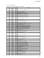
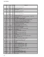
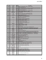
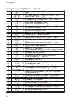
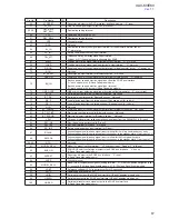
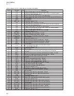
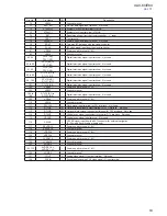
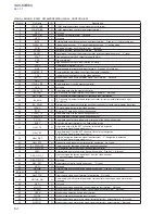
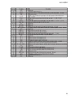
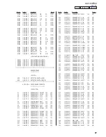
VISUAL BOARD IC2201 MN103SH23UB (VIDEO PROCESSOR)
Pin No.
Pin Name
I/O
Description
1
OSCXO
O
System clock output terminal (33 MHz)
2
OSCXI
I
System clock input terminal (33 MHz)
3 to 7
SDRA3, SDRA4,
SDRA2, SDRA5,
SDRA1
O
Address signal output to the SD-RAM
8
VSS
-
Ground terminal
9
SDRA6
O
Address signal output to the SD-RAM
10
VDD
-
Power supply terminal (+3.3V)
11, 12
SDRA0, SDRA7
O
Address signal output to the SD-RAM
13
VDDI
-
Power supply terminal (+1.2V)
14, 15
SDRA10, SDRA8
O
Address signal output to the SD-RAM
16
SDRBA1
O
Bank address signal output to the SD-RAM
17
SDRA9
O
Address signal output to the SD-RAM
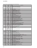
18
VSS
-
Ground terminal
19
VDD
-
Power supply terminal (+3.3V)
20
SDRBA0
O
Bank address signal output to the SD-RAM
21
SDRA11
O
Address signal output to the SD-RAM
22
NSDRCS
O
Chip select signal output to the SD-RAM
23
SDRA12
O
Address signal output to the SD-RAM
24
NSDRRAS
O
Row address select signal output to the SD-RAM
25
SDRCKE
O
Clock enable signal output to the SD-RAM
26
NSDRCAS
O
Column address select signal output to the SD-RAM
27
SDCKI
I
Clock signal input from the SDRCKO (pin 30)
28
VDD
-
Power supply terminal (+3.3V)
29
VSS
-
Ground terminal
30
SDRCKO
O
Clock signal output to the SDCKI (pin 27) and SD-RAM
31
NSDRWE
O
Write enable signal output to the SD-RAM
32
SDRDQM1
O
Data mask signal output to the SD-RAM (upper byte)
33
SDRDQM0
O
Data mask signal output to the SD-RAM (lower byte)
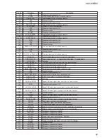
34 to 37
SDRD8, SDRD7,
SDRD9, SDRD6
I/O
Two-way data bus with the SD-RAM
38
VDD
-
Power supply terminal (+3.3V)
39
VSS
-
Ground terminal
40 to 48
SDRD10,
SDRD5, SDRD11,
SDRD4,SDRD12,
SDRD3, SDRD13,
SDRD2, SDRD14
I/O
Two-way data bus with the SD-RAM
49
VDD
-
Power supply terminal (+3.3V)
50
VSS
-
Ground terminal
51
VDDI
-
Power supply terminal (+1.2V)
52 to 54
SDRD1, SDRD15,
SDRD0
I/O
Two-way data bus with the SD-RAM
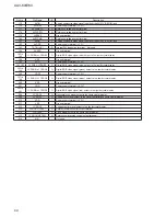
55
NRST
I
Reset signal input from the visual controller “L”: reset
56
NMI
I
Non-maskable interrupt signal input terminal Fixed at “H” in this set
57
LCDICLK
I
Clock signal input terminal Not used
58
TSTC0
I
Test signal input terminal Fixed at “L” in this set
59
TSTCK
I
Test signal input terminal Fixed at “L” in this set
60
VSS
-
Ground terminal
61, 62
TSTC1, TSTC2
I
Test signal input terminal Fixed at “L” in this set
63
PINMD1
I
Mode signal input terminal Fixed at “L” in this set
64
SDATA
I/O
Two-way data bus terminal for debug
65
VSS
-
Ground terminal
66
VDD
-
Power supply terminal (+3.3V)
67
SCLOCK
I
Clock signal input terminal for debug
68
PINMD0
I
Mode signal input terminal Fixed at “L” in this set
69
VDDI
-
Power supply terminal (+1.2V)
70, 71
NFRCS0, NFRCS1
O
Chip enable signal output to the fl ash memory
72
NFRWE
O
Write enable signal output to the fl ash memory
73
VSS
-
Ground terminal
Summary of Contents for XAV-60 - 6.1 Inch Avc
Page 92: ...92 XAV 60 E60 MEMO ...

