XDR-S40DBP
XDR-S40DBP
13
13
SECTION 4
DIAGRAMS
For Schematic Diagrams.
Note:
• All capacitors are in
μ
F unless otherwise noted. (p: pF) 50
WV or less are not indicated except for electrolytics and
tantalums.
• All resistors are in
Ω
and 1/4 W or less unless otherwise
speci
fi
ed.
•
C
: Panel designation.
THIS NOTE IS COMMON FOR PRINTED WIRING BOARDS AND SCHEMATIC DIAGRAMS.
(In addition to this, the necessary note is printed in each block.)
•
A
: B+ Line.
• Voltages are dc with respect to ground under no-signal
(detuned) conditions.
no mark : TUNER (FM)
• Voltages are taken with VOM (Input impedance 10 M
).
Voltage variations may be noted due to normal production
tolerances.
• Signal path.
F
:
AUDIO
For Printed Wiring Boards.
Note:
•
X
: Parts extracted from the component side.
•
Y
: Parts extracted from the conductor side.
•
: Pattern from the side which enables seeing.
(The other layers’ patterns are not indicated.)
• Indication of transistor.
Note:
The components identi
fi
ed by mark
0
or dotted
line with mark
0
are critical for safety.
Replace only with part number speci
fi
ed.
C
B
These are omitted.
E
Q
GND 1
VDD 2
+
–
VREF
OUT
4
CD
3
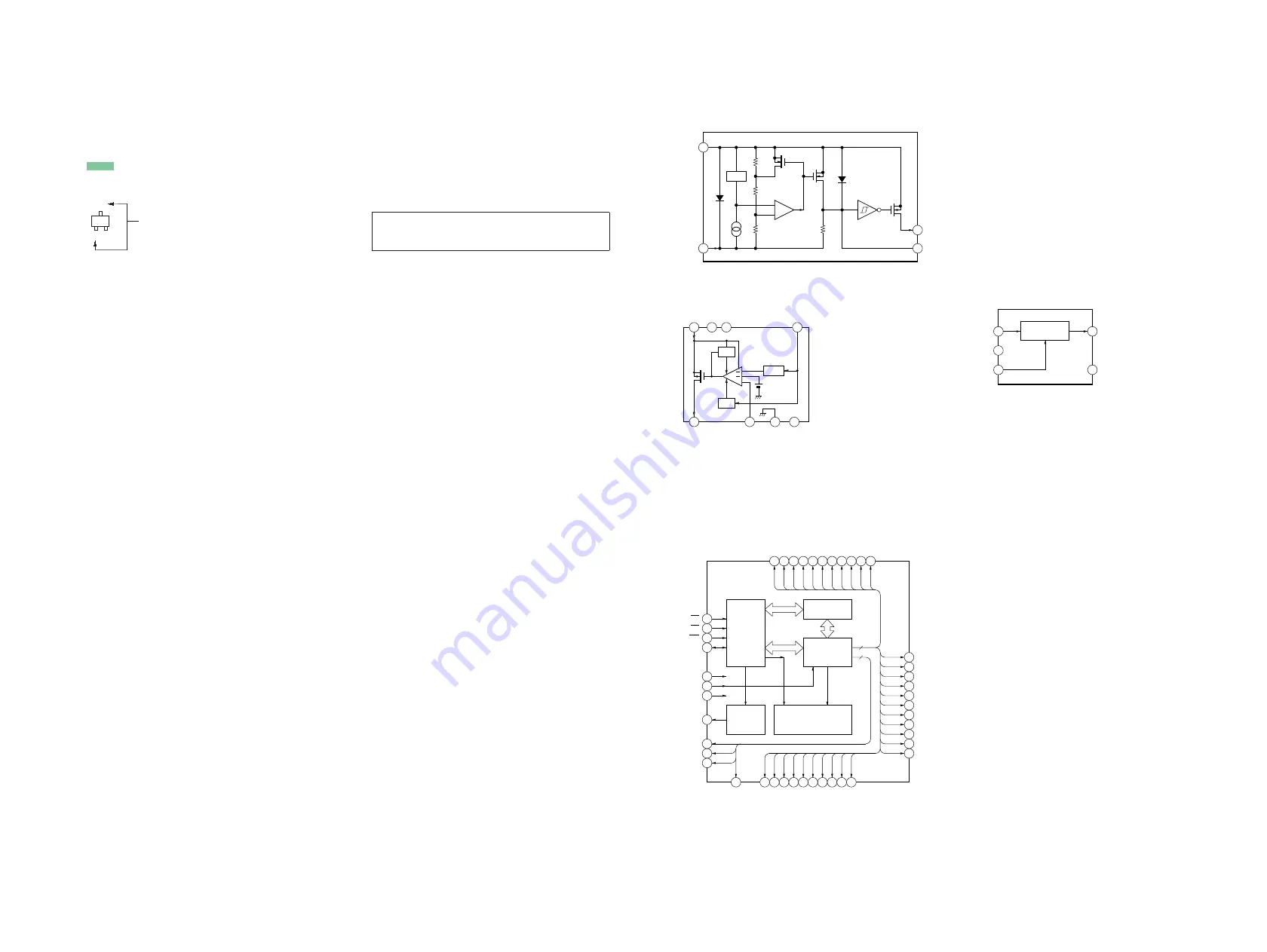
• IC Block Diagrams
– MAIN Board –
IC102 PST8436UL
IC105 MM3291CNRE
5
7
8
2
1
3
VOUT
FB
GND
4
N.C.
VCC
N.C.
6
N.C.
EN
+
SOFT
TSD
OCP
VDD 1
GND 2
CE 3
NC
4
REGULATOR
VOUT
5
CS
SEG10
1
RD 2
WR 3
DATA 4
SEG21
24
BZ 8
COM0 9
COM1 10
COM2 11
34
SEG30
14
SEG31
13
COM3
12
VSS 5
VLCD 6
VDD 7
CONTROL
AND
TIMING
SCIRCUIT
LCD DRIVER/
BASE CIRCUIT
DISPLAY
RAM
TONE
FREQUENCY
GENERATOR
WATCHDOG TIMER
AND
TIME BASE GENERATOR
SEG29
15
SEG28
16
SEG27
17
SEG26
18
SEG25
19
SEG24
20
SEG23
21
SEG22
22
SEG20
23
SEG19
25
SEG18
26
SEG17
27
SEG16
28
SEG15
29
SEG14
30
SEG13
31
SEG12
32
SEG11
33
4
32
SEG9
35
SEG8
36
SEG7
37
SEG6
38
SEG5
39
SEG4
40
SEG3
41
SEG2
42
SEG1
43
SEG0
44
IC103 BD00GA5WEFJ-E2
– LCD Board –
IC301 HT1621
Summary of Contents for XDR-S40DBP
Page 27: ...MEMO XDR S40DBP 27 ...


