background image

22

XDR-S40DBP

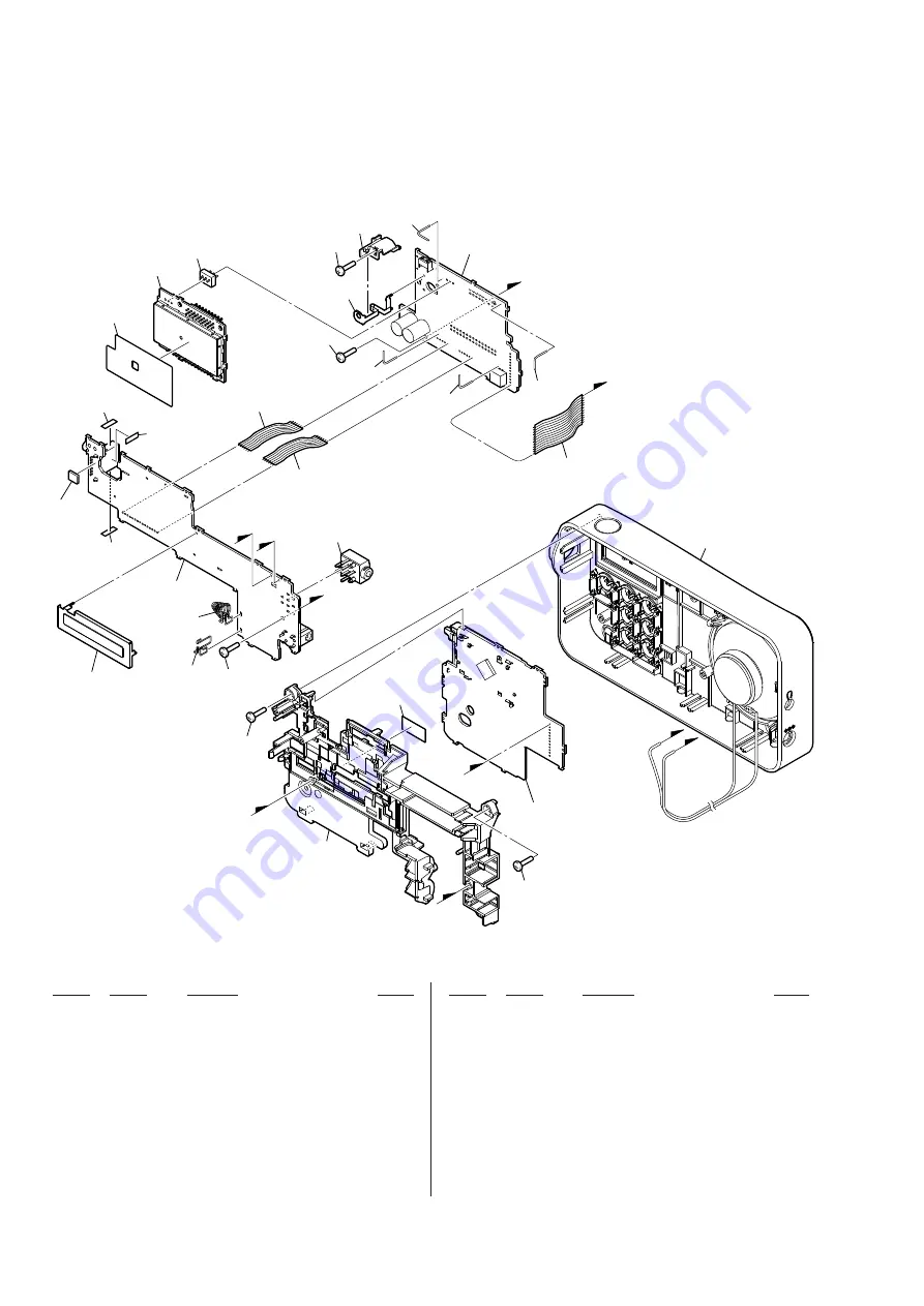
5-3.  CHASSIS  SECTION

•  Rear side view

  101 

4-437-731-01  TERMINAL (PLUS), BATTERY

  102 

4-437-732-01  TERMINAL (MINUS), BATTERY

 103 

3-254-070-01 SCREW

 104 

4-455-484-01 TERMINAL 

(MODULE)

 105 

4-437-730-01 TERMINAL, 

ANT

 106 

4-439-771-01 HOLDER 

(ANTENNA)

  107 

4-441-303-01  SHEET (INSULATING, MD)

 108 

4-437-687-01 CHASSIS

  109 

3-252-827-01  SCREW (B2.6), (+) BV TAPPING (for WHITE, RED)

  109 

3-252-827-11  SCREW (B2.6), (+) BV TAPPING (for BLACK)

 110 

4-453-876-01 SHEET 

(INSULATING, 

TERMINAL)

 111 

4-462-207-01 SHEET 

(VOL)

 CAB1  A-1904-051-A CABINET 

FRONT 

ASSY 

(Including SPEAKER, BUTTON) (for BLACK)

 CAB1  A-1908-256-A CABINET 

FRONT 

ASSY 

(Including SPEAKER, BUTTON) (for WHITE)

 CAB1  A-1908-260-A CABINET 

FRONT 

ASSY 

(Including SPEAKER, BUTTON) (for RED)

  CN104 

1-843-530-11  PIN, CONNECTOR 3P

  DAB1 

X-2587-128-1  MODULE ASSY (SVX) (DAB module)

 J202  1-785-448-21 JACK 

(

i

)

  Ref. No. 

Part No. 

Description 

Remark

  Ref. No. 

Part No. 

Description 

Remark

LCDDAB board section

110

109

103

101

102

not
supplied

not supplied

not supplied

not supplied

not supplied

DAB1

107

106

105

104

104

104

104

103

103

108

J202

CAB1

CN104

111

111

111

E

A

A B

B

C

C

D

D

E

not supplied
(JACK board)

not supplied
(MAIN board)

109

Summary of Contents for XDR-S40DBP

Page 1: ...13D 235 776 7D 194 064 11A 216 928 13E 237 488 8A 195 936 11N 217 088 13F 239 200 8B 197 648 11B 218 640 Speaker Approx 6 6 cm dia 8Ω monaural Audio power output 0 3 W Output headphones jack ø 3 5 mm stereo mini jack Power requirements 6 V DC four LR6 size AA alkaline batteries External power source DC IN 6V Battery life JEITA Approx 13 hours for DAB 10 hours for FM Using Sony LR6SG alkaline batte...

Page 2: ...viscous sticky less prone to flow than ordinary solder so use caution not to let solder bridges occur such as on IC pins etc Usable with ordinary solder It is best to use only unleaded solder but unleaded solder may also be added to ordinary solder 1 SERVICING NOTES 2 2 DISASSEMBLY 2 1 Disassembly Flow 3 2 2 Cabinet Rear Block 4 2 3 VOL Knob Block 4 2 4 Cabinet Front Assy CAB1 5 2 5 LCDDAB Board 6...

Page 3: ...e order shown below 2 1 DISASSEMBLY FLOW SET 2 2 CABINET REAR BLOCK Page 4 2 4 CABINET FRONT ASSY CAB1 Page 5 2 5 LCDDAB BOARD Page 6 2 6 JACK BOARD Page 7 2 7 MAIN BOARD BLOCK Page 8 2 8 MAIN BOARD Page 9 2 9 MODULE ASSY DAB MODULE DAB1 Page 9 2 3 VOL KNOB BLOCK Page 4 ...

Page 4: ...apping screws B2 6 3 Open the battery lid 2 telescopic antenna ANT1 ANT terminal 6 claw claw 7 cabinet rear block cabinet rear block cabinet front Rear side view Rear side view Note 4 When installing the cabinet rear block attach two claws to the cabinet front first claw ANT terminal square hole screw hole Note 2 When installing the telescopic antenna ANT1 install it on after installing the cabine...

Page 5: ...LUH VHWWLQJ 3 tapping screw B2 6 5HDU WRS VLGH YLHZ Note Wire must not run a ground into the solder portion of J201 4 Insert a flat blade screwdriver between the chassis block and the cabinet front assy lean in the direction of an arrow and remove the chassis block 7 cabinet front assy CF1 5 Remove the chassis block in the direction of an arrow 6 chassis block ...

Page 6: ... board 1 two craws 1 two craws 2 Remove the LCDDAB board in the direction of an arrow 3 Remove twelve solders MAIN board LCDDAB board LUH VHWWLQJ Note Arrange a wire in order of arrow A and arrow B A B URQW ERWWRP YLHZ URQW ERWWRP VLGH YLHZ ...

Page 7: ...ery terminal plus Rear bottom view 8 boss 9 Remove the JACK board block in the direction of an arrow Battery terminal setting Note 1 Insert only 1 turn in the ditch Note 2 When installing the JACK board lean C216 and C230 in the direction of an arrow Wire setting JACK board JACK board MAIN board flat wire MAIN board DAB module Side view Note 3 Wire must not touch the JACK board Note 4 Fix the flat...

Page 8: ...crew 1 screw 2 claw 2 claw 3 boss 5 Remove the MAIN board block in the direction of an arrow 7 MAIN board block MAIN board LCDDAB board 3 boss 4 rib 4 rib LUH VHWWLQJ Note Arrange a wire in order of arrow A and arrow B A B URQW ERWWRP VLGH YLHZ 5HDU WRS VLGH YLHZ ...

Page 9: ...AIN board 9 wire 6 core 5 Remove three solders 6 two claws 7 holder antenna block 3 Remove eighteen solders 3 Remove thirty solders 1 Remove the solder 1 Remove the solder 1 Remove the solder 1 Remove the solder 1 Remove the solder 1 Remove the solder 1 Remove the solder 1 Remove the solder 2 terminal module 2 terminal module 2 terminal module 2 terminal module 4 DAB module block terminal module M...

Page 10: ...gu lated DC power supply and outputs the voltage of 6V 2 Telescopic antenna is set and press the 1 button to turn the power on Checks that there is mark in the upper right of the liquid crystal display 3 Press and hold the 1 button while pressing the MENU button 4 Release the MENU button 1 button is holding 5 Press the v V button in order and release the 1 button Enter the test mode and the FW VER...

Page 11: ... in the clockwise direction to a maxi mum The sound from a headphone becomes large suitably and it checks that there is no defective sound quality 11 Headphone is pull out from the unit It checks that the unit is struck 3 times lightly and the sound from a speaker does not have interruption and defective sound quality 12 VOL jog is turned in the counterclockwise direction to a minimum The sound fr...

Page 12: ... there is no defective sound quality Sound is not outputted at the time of a minimum 13 VOL jog is turned in the clockwise direction to a maxi mum The sound from a headphone becomes large suitably and it checks that there is no defective sound quality 14 Headphone is pull out from the unit It checks that the unit is struck 3 times lightly and the sound from a speaker does not have interruption and...

Page 13: ...from the side which enables seeing The other layers patterns are not indicated Indication of transistor Note The components identified by mark 0 or dotted line with mark 0 are critical for safety Replace only with part number specified C B These are omitted E Q GND 1 VDD 2 VREF OUT 4 CD 3 IC Block Diagrams MAIN Board IC102 PST8436UL IC105 MM3291CNRE 5 7 8 2 1 3 VOUT FB GND 4 N C VCC N C 6 N C EN S...

Page 14: ...JL102 JL103 JL104 C120 C121 JL105 C122 JL106 JL107 C123 JL108 C124 JL109 C125 C126 C128 C129 JL110 C134 C136 C137 C138 C139 C140 C142 C143 C144 C145 C146 C147 C148 C149 C150 D102 D103 D104 D105 IC101 IC102 IC103 IC104 IC105 IC106 1 2 4 3 1 12 6 1 6 1 W102 W103 W101 CN101 CN102 CN103 S101 C127 C132 JW101 JW102 JW103 JW104 JW105 JW106 JW107 JW108 JW109 JW110 JW111 JW112 JW113 JW114 JW115 JW116 JW117...

Page 15: ...L IC104 1 OUT 2 VDD 3 NC 4 VSS DA2J10100L D104 PST8436UL IC102 1 GND 2 VDD 3 CD 4 OUT 1M R141 1 C138 0 1 C137 DA2J10100L D103 470k R137 CL108 1 C144 CL107 S SSM3J15FU T5LSOY E Q102 0 01 C136 PST8218UL IC101 1 VOUT 2 VDD 3 NC 4 VSS 4 7k R131 1k R130 470k R140 JL105 JL103 100k R129 10k R101 10k R102 0 1 C139 100k R106 0 1 C104 1000p C111 SL101 CL110 1000p C134 JL102 0 R145 0 R144 CL115 CL116 CL117 C...

Page 16: ...6 JL218 JL219 CL203 CL201 R249 R251 R252 R261 R262 C232 R270 C235 R273 C242 C243 D204 IC202 CL202 F201 CL227 Q201 Q202 SL203 Q213 Q214 Q220 5 8 4 1 1 6 1 6 JW206 JW228 JW227 JW222 JW221 JW220 JW219 JW218 JW217 JW216 JW211 JW209 J202 JW208 C216 C217 C230 C233 C234 C236 C237 JW201 JW202 JW203 JW204 JW205 D205 JW212 JW213 JW214 JW215 JW230 IC204 JW231 RV201 W201 W203 J201 A K K A 1 3 2 1 7 S G D D S ...

Page 17: ...1 20k RV201 1 2 3 4 5 6 7 JL218 1k R245 JL201 JL202 10k R202 DA2J10100L D204 1 C235 CL203 16V C216 470 2 2k R225 2 2k R224 10k R223 DA2J10100L D208 J202 0 01 C240 0 01 C241 SL201 470k R249 470k R243 2SC4081T106Q Q213 S SSM3J305T T5LSOY E Q214 10V 1000 C230 100k R247 S SSM3K15FU TE85L Q218 S SSM3K15FU TE85L Q217 CL221 CL220 CL219 CL216 CL217 CL214 CL215 CL218 CL223 CL224 CL225 CL226 SL202 50V 1A F2...

Page 18: ...32 JL333 JL334 JL335 JL336 JL337 JL338 JL339 JL340 JL341 JL342 JL343 JL344 JL345 JL346 JL347 JL348 1L0341Y22C0TT001 D301 R304 100 R305 220 R326 4 7k 100k R361 220k R360 LTA043TUBFS8TL Q305 LTC015EUBFS8TL Q303 S SSM3K15FU TE85L Q302 470k R306 CL300 CL302 CL301 C307 1 C308 1 C303 0 1 C302 0 1 SEG 0 SEG 1 SEG 2 SEG 3 SEG 4 SEG 5 SEG 6 SEG 7 SEG 8 SEG 9 SEG 10 SEG 11 SEG 12 SEG 13 SEG 14 SEG 15 SEG 16...

Page 19: ...JL334 JL336 JL318 JL320 JL322 JL316 JL314 JL325 JL327 JL329 JL331 JL333 JL335 JL337 JL338 JL340 JL342 JL344 JL339 JL341 JL343 JL345 JL346 JL348 JL347 JW304 W301 S301 S303 S302 S304 S306 S305 S307 JW301 JW302 JW303 JW305 JW306 D301 11 1 12 34 44 22 23 33 12 1 E S G S G D D E S301 307 1 734 130 11 11 MENU v BACK PRESET LCDDAB BOARD LCD1 LIQUID CRYSTAL DISPLAY V ENTER DISP DAB FM LCD BACK LIGHT SHIEL...

Page 20: ...56 21 ANTENNA TELESCOPIC Ref No Part No Description Remark Ref No Part No Description Remark Note XX and X mean standardized parts so they may have some difference from the original one Items marked are not stocked since they are seldom required for routine ser vice Some delay should be anticipated when ordering these items The mechanical parts with no reference number in the exploded views are no...

Page 21: ...437 685 21 CABINET REAR for WHITE RED 54 4 142 819 01 BATTERY TERMINAL B 55 4 142 818 01 BATTERY TERMINAL A 56 4 459 425 01 CUSHION BATTERY CASE LID A for BLACK 56 4 459 425 11 CUSHION BATTERY CASE LID A for WHITE RED 57 4 459 426 01 CUSHION BATTERY CASE LID B for BLACK 57 4 459 426 11 CUSHION BATTERY CASE LID B for WHITE RED Ref No Part No Description Remark Ref No Part No Description Remark 51 5...

Page 22: ... 462 207 01 SHEET VOL CAB1 A 1904 051 A CABINET FRONT ASSY Including SPEAKER BUTTON for BLACK CAB1 A 1908 256 A CABINET FRONT ASSY Including SPEAKER BUTTON for WHITE CAB1 A 1908 260 A CABINET FRONT ASSY Including SPEAKER BUTTON for RED CN104 1 843 530 11 PIN CONNECTOR 3P DAB1 X 2587 128 1 MODULE ASSY SVX DAB module J202 1 785 448 21 JACK i Ref No Part No Description Remark Ref No Part No Descripti...

Page 23: ...DAB SHIELD 152 4 437 733 01 SHEET DIFFUSION 153 4 450 048 01 CUSHION LIGHT GUIDE PLATE 154 4 437 692 01 PLATE LIGHT GUIDE 155 4 437 691 01 LCD HOLDER DAB D301 6 501 601 01 LED 1L0341Y22C0TT001 LCD BACK LIGHT LCD1 1 811 737 11 DISPLAY PANEL LIQUID CRYSTAL Ref No Part No Description Remark Ref No Part No Description Remark ...

Page 24: ...206 1 216 821 11 METAL CHIP 1K 5 1 10W R207 1 216 853 11 METAL CHIP 470K 5 1 10W R209 1 216 853 11 METAL CHIP 470K 5 1 10W R215 1 216 845 11 METAL CHIP 100K 5 1 10W R221 1 216 821 11 METAL CHIP 1K 5 1 10W R222 1 216 853 11 METAL CHIP 470K 5 1 10W R223 1 216 833 11 METAL CHIP 10K 5 1 10W R224 1 216 825 11 METAL CHIP 2 2K 5 1 10W R225 1 216 825 11 METAL CHIP 2 2K 5 1 10W R226 1 216 853 11 METAL CHIP...

Page 25: ...L CHIP 100K 5 1 10W SWITCH S301 1 554 937 11 SWITCH KEY BOARD MENU S302 1 554 937 11 SWITCH KEY BOARD BACK S303 1 554 937 11 SWITCH KEY BOARD v S304 1 554 937 11 SWITCH KEY BOARD ENTER DISP S305 1 554 937 11 SWITCH KEY BOARD PRESET S306 1 554 937 11 SWITCH KEY BOARD DAB FM S307 1 554 937 11 SWITCH KEY BOARD V MAIN BOARD 4 437 730 01 TERMINAL ANT 4 439 771 01 HOLDER ANTENNA 4 441 303 01 SHEET INSUL...

Page 26: ... 216 845 11 METAL CHIP 100K 5 1 10W R130 1 216 821 11 METAL CHIP 1K 5 1 10W R131 1 216 829 11 METAL CHIP 4 7K 5 1 10W R133 1 216 849 11 METAL CHIP 220K 5 1 10W R134 1 216 864 11 SHORT CHIP 0 R136 1 216 825 11 METAL CHIP 2 2K 5 1 10W R137 1 216 853 11 METAL CHIP 470K 5 1 10W R139 1 216 845 11 METAL CHIP 100K 5 1 10W R140 1 216 853 11 METAL CHIP 470K 5 1 10W R141 1 216 857 11 METAL CHIP 1M 5 1 10W R...

Page 27: ...MEMO XDR S40DBP 27 ...

Page 28: ...N HISTORY Checking the version allows you to jump to the revised page Also clicking the version at the top of the revised page allows you to jump to the next revised page Ver Date Description of Revision 1 0 2013 01 New ...

Reviews: