6-6.
Frame Memory Section
6-6-1.
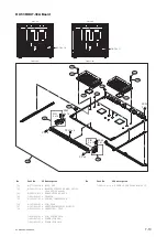
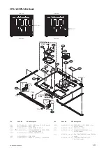
VPR-129 Board (XKS-8440)
The VPR-129 board has the following functions.
• Stores video signals from SDI_IN in the DDR memory on this board and then stores them in the internal SSD.
• Expands stored images in the DDR memory in the same was as input signals, and then outputs them to SDI_OUT.
• SDI_IN supports 8 channels and SDI_OUT supports 20 channels.
• Imports and exports video clip with external devices through the Ethernet.
Function of the FPGA (IC1)
Input of the SDI signal
Serial-to-parallel conversion is made for 8-channel SDI signals that are input from CNP1. Then the parallel DI signals
are stored in the in the DDR memory on the board, and are then sent to the CPU (IC3) through PCIex4.
SDI output
The video clip sent from the CPU through PCIex4 is stored in the DDR memory on the board, and is then converted to
a serial signal. Then the serial signal is output from CNP1, CNL1, and CNE1 as SDI signal for up to 20 channels.
DDR control
The DDR memory is used to adjust timing between SDI signal and PCIe signal. The DDR memory consists of four
8GB_DIMM devices.
Function of the CPU (IC3)
SSD control
This CPU stores and manages the SDI input signal or the video clip imported from the external device in the internal
SSD. The stored video clip is sent to the FPGA through PCIe or is exported to external devices upon instructions from
the upper CPU.
Ethernet communication
This CPU performs communication with the upper CPU to control Clip Store, and also imports and exports video clip
from/to external devices through this Ethernet communication.
DDR control
This CPU manages and controls the DDR address for timing adjustment between SSD and PCIe.
i2c Bus control
This CPU performs communication with the board temperature monitoring IC (IC3304), real-time clock (IC3306), and
the NVRAM (IC3305, IC3306).
SD-CARD
This CPU is connected to the maintenance SD-CARD for system firmware download. This CPU is booted from this
SD-CARD at the time of maintenance.
Function of the CADEC (IC2)
Configuration of the FPGA
When the board is turned on, this CADEC configures the FPGA (IC1) by using the configuration data stored in the
FLASH_ROM (IC1902) and makes initial settings.
Startup of the CPU
After the FPGA configuration has been completed, this CADEC releases the CPU reset. The CPU runs with the boot
data and application data in the FLASH_ROM (IC1901).
Communication between CPU and FPGA
The CPU reads and writes registers of the FPGA through the CADEC, and decodes addresses to access registers.
XVS-8000-C/XVS-8000
6-10

