background image

9

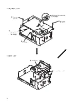
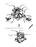
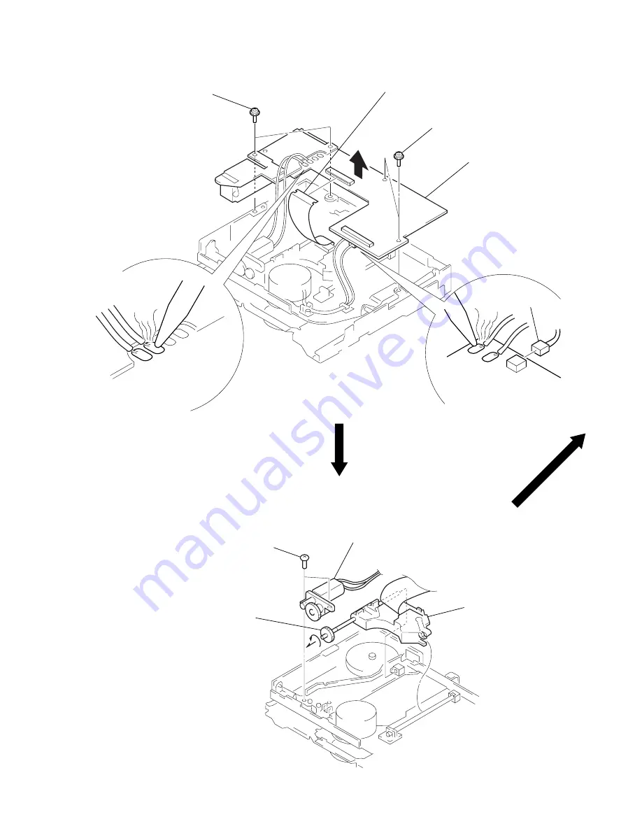
RF  BOARD

SLED  MOTOR  ASS’Y (M102),  OPTICAL  PICK-UP (KSS-521A/J2N)

4

3

two screws
(PS2 

×

 4)

5

connector
(CNP53)

7

RF board

3

two screws
(PS2 

×

 4)

1

OP flexible board
(CNJ11)

2

Break the soldering 
of motor (M102) lead.

6

Break the soldering of lead.

1

two screws
(ESCUTCHEON)

4

Turn at the direction of the 
arrow, then remove 
shaft (sled) ass’y

2

sled motor ass’y
(M102)

3

optical pick-up
(KSS-521A/J2N)

Summary of Contents for Xplod CDX-737

Page 1: ...VICE MANUAL COMPACT DISC CHANGER SPECIFICATIONS CDX 737 US Model Canadian Model AEP Model UK Model E Model Model Name Using Similar Mechanism NEW CD Drive Mechanism Type MG 250D 137 Optical Pick up Name KSS 521A J2N ...

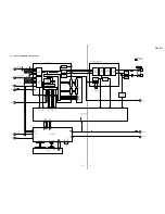
Page 2: ...B LISHED BY SONY TABLE OF CONTENTS 1 SERVICING NOTES 3 2 GENERAL 3 Installation 4 Connections 4 3 DISASSEMBLY 5 4 MECHANISM DECK ASSEMBLY 11 5 MECHANICAL ADJUSTMENTS 13 6 ELECTRICAL ADJUSTMENTS 14 7 DIAGRAMS 7 1 Block Diagram SERVO Section 16 7 2 Block Diagram MAIN Section 17 7 3 Block Diagram BUS CONTROL POWER SUPPLY Section 18 7 4 Note for Printed Wiring Boards and Schematic Diagrams 19 7 5 Prin...

Page 3: ...ents or performance of procedures other than those specified herein may result in hazardous ra diation exposure Flexible Circuit Board Repairing Keep the temperature of the soldering iron around 270 C dur ing repairing Do not touch the soldering iron on the same conductor of the circuit board within 3 times Be careful not to apply force on the conductor when soldering or unsoldering Notes on chip ...

Page 4: ...4 4 ...
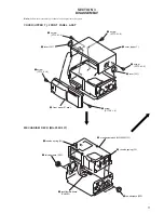
Page 5: ...EL ASS Y MECHANISM DECK MG 250D 137 1 screw PTT2 6 6 1 screw PTT2 6 6 2 cover upper T 1 screw PTT2 6 6 1 screw PTT2 6 6 1 screw PTT2 6 6 3 lever FLT 3 lever FLT 4 front panel T ass y 2 tension spring FL 2 tension spring FL 1 two dampers 250 1 two dampers 250 3 jack flexible board CNJ901 4 mechanism deck MG 250D 137 ...

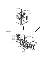
Page 6: ...k board in the direction of the arrow 1 ground point screw PTT2 6 6 2 jack board 1 main flexible board CNJ12 6 three screws FP 7 main board 2 Break the soldering of motor M104 lead 3 screw PTT2 4 4 heat sink 5 two precision screws P1 7 2 5 ...

Page 7: ...TT2 3 2 bracket EVM 3 elevator motor ass y M104 2 Remove the claw in the direction of the arrow A 4 Remove the ditch in the direction of the arrow B A B 5 Remove the escutcheon in the direction of the arrow C 4 ditch 3 claw C 3 two claws 1 screw M2 3 ...

Page 8: ... ASS Y 1 three screws PTT2 4 1 two screws PTT2 4 2 4 Remove the case upper ass y in the direction of the arrow B 3 Remove the edge in the direction of the arrow A 1 screw PTT2 4 A B 3 chassis ass y 1 two polyethylene washers 2 2 ...

Page 9: ...connector CNP53 7 RF board 3 two screws PS2 4 1 OP flexible board CNJ11 2 Break the soldering of motor M102 lead 6 Break the soldering of lead 1 two screws ESCUTCHEON 4 Turn at the direction of the arrow then remove shaft sled ass y 2 sled motor ass y M102 3 optical pick up KSS 521A J2N ...

Page 10: ...ews P1 7 2 2 7 3 spring chucking 6 retainer disc 4 screw P2 2 2 5 bracket CP 9 Remove the spindle motor ass y M101 in the direction of the arrow 2 SW board 1 screw P2 2 2 1 Break the soldering of motor M103 lead 2 two screws P2 2 5 4 chucking motor ass y M103 3 retainer CHM ...

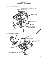
Page 11: ...e the chuck plate is moved down to the lower limit A B 4 stop ring 2 0 E type 5 tension spring DH 2 washer 2 5 3 optical pick up complete ass y Note Insert the shaft A first shaft A gear LOAD 2 gear LOMINI marking Fig A chuck plate 2 Attach the gear LOMINI at the position shown in Fig A shaft rotary prevention C 1 Move the lever LOCK 3 fully in direction B to move the chuck plate up B 4 stop ring ...

Page 12: ... moves in direction C to move down the chuck plate if the gear LOAD CAM is rotated in direction A or the chuck plate moves up and the slider moves in direction D if the gear is rotated in direction B chuck plate slider gear LOAD CAM ass y A B C D ...

Page 13: ...s 5 and 6 as shown below adjust the following 5 Press repeatedly the DISC and buttons on the master unit so that the elevator shaft moves from address 6 to address 5 or from 5 to 6 At this time adjust RV201 on the main board so that the elevator shaft positions smoothly between comb teeth A and B 6 Further place the set horizontally and make same adjustment as mentioned above 7 After adjustment at...

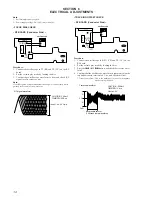
Page 14: ...OFFSET CHECK RF BOARD Conductor Side Procedure 1 Connect the oscilloscope to BP11 TE and TP VC on the RF board 2 Put the set into play mode by loading the disc 3 Press the AMS button and check the traverse wave form 4 Confirm that the oscilloscope waveform is symmetrical on the top and bottom in relation to 0 V dc and check this level Traverse waveform This is the tracking error wave form appears ...

Page 15: ...2 Check that there is not an abnormal amount of operation noise white noise from the 2 axis devise If there is turn RV14 slightly clockwise RF BOARD Conductor Side When gain is lowered The set does not play because of no focus operation When gain is highered Operation noise is heard due to a scratch or a dust then opera tion will be unstable RV14 IC11 IC51 CNJ12 MIN side low gain MAX side high gai...

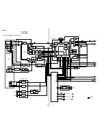
Page 16: ...7 17 16 6 25 24 13 PD1 PD1 I V AMP RFO RF 46 ASYI 47 ASYO FOK DATO CLKO XLTO SEIN CNIN C OUT FOK SUBQ SCLK SENS CD DATA CD CLK CD XLT SCOR MON MDP MDS 29 LOCK 64 SQSO SQCK SENS DATA CLOCK XLAT SCOR SBSO EXCK GFS GTOP WFCK EMPH C4M XRST RFI FOK DATA CLK SENS1 26 SENS2 C OUT XLT LOCK XRST PD2 I V AMP PD2 TTL IIL FEO TEO PD FEI FEO TAO TEI TTL IIL TTL IIL FOCUS ERROR AMP RF SUMMING AMP TRACKING ERROR...

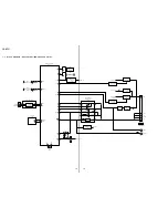
Page 17: ...IC501 D RAM IC402 S RAM IC502 A0 A9 D1 D4 XTAI TIMING GENERATOR D A CONVERTER INTERFACE SERIAL INPUT INTERFACE TIMING GENERATOR CPU INTERFACE OSC MUTING CONTROL SWITCH Q601 602 MUTING Q610 LOW PASS FILTER DIGITAL FILTER CIRCUIT Σ MODULATOR CIRCUIT DATA D OUT BCK LRCK DATA BCK LRCK MCK D RAM CONTROLLER IC401 DIGITAL OUT Page 16 D SCLK IC503 SBSO Page 16 E Page 16 G SCOR Page 16 F DATA CLOCK Page 16...

Page 18: ... D308 D306 9V REGULATOR Q309 REGULATOR CONTROL SWITCH Q308 REGULATOR CONTROL SWITCH Q306 REFERENCE VOLTAGE SWITCH Q201 LINEAR POSITION SENSOR SERVO 9V D311 12 1 4 11 9 6 10 M 1 7 4 5 70 58 ELV R ELV F ELEVATOR MOTOR DRIVE EEPROM IC202 ELEVATOR MOTOR DRIVE IC301 FIN RIN 5 6 12 11 EE DATA EE CLK SDA SCL OUT1 OUT2 M104 ELEVATOR ELV ON MCK RV201 ELEVATOR HEIGHT SENSOR RV202 38 EHS 39 AVREF 37 RESET SW...

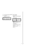
Page 19: ...or less unless otherwise specified f internal component C panel designation U B Line H adjustment for repair Power voltage is dc 14 4V and fed with regulated dc power supply from CD changer controller Voltages and waveforms are dc with respect to ground under no signal conditions no mark CD PLAY Impossible to measure Voltages are taken with aVOM Input impedance 10 MΩ Voltage variations may be note...

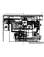
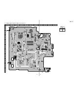
Page 20: ...2 R16 C40 R28 C23 R33 R12 R13 B C E C13 CNJ11 Q11 1 676 014 11 11 RF BOARD CONDUCTOR SIDE IC51 CNJ12 SW1 LIMIT SW BOARD 1 664 104 11 11 M101 SPINDLE A MAIN BOARD OPTICAL PICK UP BLOCK KSS 521A OP FLEXIBLE BOARD 1 664 626 11 SW11 CHUCKING END DETECT SW12 SAVE END DETECT 1 2 3 4 5 6 7 8 9 10 11 A B C D E F G H I J 1 2 BLU YEL YEL BLU 8 5 1 4 17 1 39 27 40 52 1 13 14 26 1 26 14 8 7 1 28 22 21 15 M MA...

Page 21: ...r IC Block Diagrams The components identified by mark 0 or dotted line with mark 0 are critical for safety Replace only with part number specified Les composants identifiés par une marque 0 sont critiques pour la sécurité Ne les remplacer que par une pièce portant le numéro spécifié Page 24 ...

Page 22: ...203 R202 Q201 C501 C503 IC503 C504 R504 C502 R502 R501 X501 1 20 21 40 41 60 80 1 14 15 28 IC502 IC501 R207 C202 R213 R219 R505 D306 K A D501 C201 IC401 C205 R221 C203 C401 K A D320 61 MAIN BOARD COMPONENT SIDE M M104 ELEVATOR B JACK BOARD CNJ901 05 1 674 306 12 12 1 2 3 4 5 6 7 8 9 10 11 A B C D E F G H I J C1 B2 C2 E1 B1 E2 C1 B2 C2 E1 B1 E2 BLU RED A K K A A K K K A K A 3 1 2 IC101 81 K A A 4 5...

Page 23: ...on Q307 E 11 Q309 G 11 CHASSIS CHASSIS RV202 ELEVATOR HEIGHT SENSOR RV201 UP DOWN X201 X601 SW202 MAGAZINE IN OUT DETECT C601 C609 C604 C610 C630 C620 C318 C317 C310 C314 C316 C309 Q309 Q307 SW301 Z 05 MAIN BOARD CONDUCTOR SIDE 1 674 306 12 12 1 2 3 4 5 6 7 8 9 10 11 A B C D E F G H I J CHASSIS SW201 MAGAZINE DETECT ...

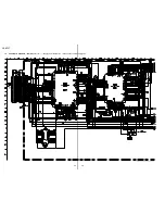
Page 24: ...24 24 CDX 737 7 9 SCHEMATIC DIAGRAM MAIN Board 1 2 See page 27 for Waveforms See page 30 for IC Block Diagrams Page 21 ...

Page 25: ...25 25 CDX 737 7 10 SCHEMATIC DIAGRAM MAIN Board 2 2 See page 28 for Waveforms See page 31 for IC Block Diagrams Page 26 ...

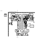
Page 26: ...Board IC901 6 8 3 2 1 7 5 4 5 4 8 7 6 2 1 3 CONTROL FOR SONY BUS L R AUDIO OUT CN901 JACK BOARD CONDUCTOR SIDE 1 674 307 12 12 05 FB901 C904 FB902 FB903 1 13 CNJ901 C901 C902 B MAIN BOARD JACK BOARD COMPONENT SIDE JACK FLEXIBLE BOARD 1 676 340 11 1 674 307 12 12 05 Page 25 Page 22 ...

Page 27: ... IC101 rl WDCK 4 IC101 t LRCK 5 IC101 tf BCKO 6 IC101 ys RFCK 7 IC101 u C4M 8 IC101 uf WFCK 9 IC101 il XTAI 0 IC201 ea EXTAL 1 4 Vp p Approx 110 mVp p Approx 280 mVp p MAIN Board 1 2 1 IC101 wj MDP CD PLAY 2 5 Vp p 7 6 µs 6 5 Vp p 119 ns 6 3 Vp p 11 4 µs 6 2 Vp p 22 7 µs 6 5 Vp p 474 ns 6 4 Vp p 13 6 µs 6 3 Vp p 119 ns 136 µs 5 8 Vp p 6 2 Vp p 59 4 ns 4 9 Vp p 124 ns ...

Page 28: ...C401 qh XTAI w IC401 qj BCK wa IC401 ql LRCK ws IC601 qd MCK wd IC601 qg XI wf IC601 wd BCK wg IC601 wf LRCK 3 1 Vp p 100 ns 5 8 Vp p 136 µs 5 8 Vp p 136 µs 6 4 Vp p 136 µs 6 5 Vp p 474 ns 6 3 Vp p 22 7 µs 6 9 Vp p 11 3 µs 6 4 Vp p 59 4 ns 6 2 Vp p 474 ns 5 6 Vp p 22 7 µs 5 8 Vp p 59 4 ns 2 5 Vp p 59 4 ns 474 ns 6 2 Vp p 22 7 µs 5 6 Vp p 6 3 Vp p 119 ns ...

Page 29: ...19 18 17 16 15 14 40 41 42 43 44 45 46 47 48 49 50 51 52 39 PD 1 I V AMP 38 PD AMP 37 LD AMP LASER POWER CONTROL FOCUS BIAS WINDOW COMPARATOR FOCUS ERROR AMP F I V AMP E I V AMP TGFL TRACKING GAIN WINDOW COMPARATOR E F BALANCE WINDOW COMPARATOR ATSC WINDOW COMPARATOR TZC COMPARATOR TRACKING PHASE COMPENSATION CENTER VOLTAGE GENERATOR FZC COMPARATOR FOCUS PHASE COMPENSATION CHARGE UP FSET ISET IIC ...

Page 30: ...70 69 68 67 66 65 64 63 62 61 60 59 58 57 56 55 54 53 52 51 80 79 78 77 76 75 74 73 72 ASYMMETRY CORRECTOR DIGITAL PLL CLOCK GENERATOR D A INTERFACE DIGITAL CLV SUB CODE PROCESSOR TIMING LOGIC CPU INTERFACE SERVO AUTO SEQUENCER ERROR CORRECTOR 16K RAM DIGITAL OUT OSC EFM DEMODULATOR TES6 VDD VSS EXCK SBSO SCOR WFCK TES5 EMPH DOUT C4M FSTT XTSL MNT0 MNT1 MNT3 XROF C2PO RFCK GFS XPCK XUGF GTOP VDD V...

Page 31: ...TA IN BUS RESET BUS DATA VREF BUS CLK GND BUS ON IN BUS ON OUT RESET RESET SWITCH VWA ADDRESS MONITOR WRITE BASE COUNTER READ BASE COUNTER CPU I F SELECTOR TIMING GEN DSP I F DATA LINKING CONTROL DAC I F DIGITAL OUT 1 2 3 4 5 6 7 8 9 10 20 19 18 17 16 15 14 13 12 11 21 22 23 24 25 26 27 28 29 30 31 32 33 34 35 36 37 38 39 40 41 42 43 44 45 46 56 55 54 53 52 51 50 49 48 47 57 58 59 60 61 62 63 64 X...

Page 32: ... 1 A14 2 3 4 5 A5 A12 A7 A6 26 A13 25 A8 24 23 A11 A9 I O GATE COLUMN DECODER BUFFER 6 A4 7 8 9 10 A0 A3 A2 A1 27 28 VCC WE 22 OE 21 A10 BUFFER 18 I O7 17 I O6 16 I O4 I O5 19 I O8 15 I O BUFFER 11 12 13 I O3 I O1 I O2 20 CE 14 GND LEVEL SHIFT LEVEL SHIFT LEVEL SHIFT DIGITAL FILTER CIRCUIT ATTENUATOR OPERATIONAL CIRCUIT DEEMPHASIS FILTER CIRCUIT D MODULATION CIRCUIT INTERFACE CIRCUIT TEST CIRCUIT ...

Page 33: ...gnal output to the CXD2522Q IC401 L reset 26 XQOK O Subcode Q OK pulse signal output to the CXD2522Q IC401 L active 27 SDTI I ESP status signal input from the CXD2522Q IC401 28 XSOE O ESP status read enable signal output to the CXD2522Q IC401 L active 29 ESPXLT O ESP latch pulse signal output to the CXD2522Q IC401 L active 30 RST I System reset signal input from the SONY bus interface IC302 and re...

Page 34: ... CXD2530Q IC101 64 EJECT I Eject switch SW301 input terminal H active 65 CD CLK O Serial data transfer clock signal output to the CXD2530Q IC101 and CXD2522Q IC401 66 CD XLT O Serial data latch pulse signal output to the CXD2530Q IC101 67 CD DATA O Serial data output to the CXD2530Q IC101 and CXD2522Q IC401 68 CD ON O D A converter and servo section power supply on off control signal output H powe...

Page 35: ... signal generator IC304 L reset For several hundreds msec after the power supply rises L is input then it changes to H 29 EXTAL I System clock input terminal 10 MHz 30 XTAL O System clock output terminal 10 MHz 31 VSS Ground terminal 32 to 55 NC O Not used open 56 BUSY O Busy signal output to the system controller IC201 L busy status 57 to 61 NC O Not used open 62 CE O Chip enable signal output to...

Page 36: ...dication of Appearance Parts Example KNOB BALANCE WHITE RED Parts Color Cabinet s Color Ref No Part No Description Remark Ref No Part No Description Remark 1 3 010 104 01 DAMPER 250 2 3 036 546 71 COVER LOWER T 3 1 664 628 11 JACK FLEXIBLE BOARD 4 1 674 307 12 JACK BOARD 5 X 3378 115 1 DOOR T ASSY 6 3 376 464 11 SCREW PTT 2 6X6 GROUND POINT 7 3 039 239 31 PANEL T FRONT 8 3 012 388 01 SCREW M2X3 9 ...

Page 37: ...MG 250D 137 3 3 3 51 52 54 53 Ref No Part No Description Remark Ref No Part No Description Remark 51 X 3375 497 1 CHASSIS U SUB ASSY 52 3 024 161 01 SPRING SUT 53 4 965 759 01 WASHER POLYETHYLENE 54 3 011 997 01 SPRING STOPPER LOWER ...

Page 38: ...D 137 Ref No Part No Description Remark Ref No Part No Description Remark 101 3 024 170 01 SPRING SB TENSION 102 3 024 172 01 BRACKET EVM 103 X 3378 136 1 CHASSIS D D SUB ASSY M104 A 3301 123 A ELJ MOTOR ASSY ELEVATOR 102 101 103 M104 12 ...

Page 39: ...9 01 GEAR NWL 156 3 010 255 01 ARM NSW 157 3 573 936 00 STOPPER REEL 158 X 3373 552 1 GEAR LOAD CAM ASSY 159 3 010 252 01 ROLLER CRE 160 3 010 268 01 SPRING DH TENSION 161 A 3290 194 I MAIN ASSY CHASSIS EVY 162 3 010 254 01 SHAFT ROTARY PREVENTION C 163 3 010 253 01 GEAR ML 164 3 701 438 11 WASHER 2 5 166 A 3317 993 A RF BOARD COMPLETE M103 A 3301 123 A ELJ MOTOR ASSY CHUCKING 163 162 161 160 159 ...

Page 40: ...01 077 A BASE OPT J ASSY 210 1 664 626 11 OP FLEXIBLE BOARD 0211 8 820 010 06 OPTICAL PICK UP KSS 521A J2RP 212 3 010 262 01 DETENT SLED M101 A 3291 956 B MOTOR SUB ASSY SPINDLE M102 A 3291 955 A MOTOR SUB ASSY SLED 208 206 205 204 203 202 201 212 211 207 209 M101 210 not supplied not supplied 10 5 5 M102 9 7 The components identified by mark 0 or dotted line with mark 0 are critical for safety Re...

Page 41: ...T 47uF 20 16V C311 1 164 346 11 CERAMIC CHIP 1uF 16V C314 1 124 589 11 ELECT 47uF 20 16V C315 1 163 038 00 CERAMIC CHIP 0 1uF 25V C316 1 115 466 00 ELECT 1000uF 20 16V C317 1 135 612 61 ELECT 100uF 20 16V C318 1 135 612 61 ELECT 100uF 20 16V C320 1 163 038 00 CERAMIC CHIP 0 1uF 25V C321 1 163 038 00 CERAMIC CHIP 0 1uF 25V C401 1 163 038 00 CERAMIC CHIP 0 1uF 25V C402 1 163 038 00 CERAMIC CHIP 0 1u...

Page 42: ...W R104 1 216 061 00 METAL CHIP 3 3K 5 1 10W R105 1 216 061 00 METAL CHIP 3 3K 5 1 10W R106 1 216 073 00 METAL CHIP 10K 5 1 10W R107 1 216 121 00 RES CHIP 1M 5 1 10W R108 1 216 097 00 RES CHIP 100K 5 1 10W R109 1 216 073 00 METAL CHIP 10K 5 1 10W R110 1 216 073 00 METAL CHIP 10K 5 1 10W R111 1 216 049 11 RES CHIP 1K 5 1 10W R114 1 216 049 11 RES CHIP 1K 5 1 10W R202 1 216 097 00 RES CHIP 100K 5 1 1...

Page 43: ...00 CERAMIC CHIP 0 0068uF 10 50V C52 1 163 038 00 CERAMIC CHIP 0 1uF 25V C53 1 163 038 00 CERAMIC CHIP 0 1uF 25V C54 1 163 038 00 CERAMIC CHIP 0 1uF 25V C55 1 163 023 00 CERAMIC CHIP 0 015uF 5 50V C56 1 163 038 00 CERAMIC CHIP 0 1uF 25V C57 1 163 038 00 CERAMIC CHIP 0 1uF 25V C58 1 163 038 00 CERAMIC CHIP 0 1uF 25V C59 1 163 038 00 CERAMIC CHIP 0 1uF 25V C60 1 104 914 11 TANTALUM CHIP 22uF 20 16V C...

Page 44: ...M102 A 3291 955 A MOTOR SUB ASSY SLED M103 A 3301 123 A ELJ MOTOR ASSY CHUCKING M104 A 3301 123 A ELJ MOTOR ASSY ELEVATOR HARDWARE LIST 1 7 627 852 07 SCREW PRECISION P 1 7X2 5 2 7 685 792 09 SCREW PTT 2 6X6 S 3 7 685 781 09 SCREW PTT 2X4 S 4 7 624 104 04 STOPRING 2 0 TYPE E 5 7 627 554 07 SCREW PRECISION P 2X2 2 6 7 628 253 00 SCREW PS 2X4 7 7 627 553 27 SCREW PRECISION P 2X2 5 8 7 624 102 04 STO...

Reviews: