39
ZS-H10CP/H20CP
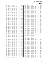
Pin No.
Pin Name
I/O
Description
47
I-VM
I
Input terminal for battery middle point voltage detection
48
I-SHIMUKE
I
Input terminal for destination discrimination
49, 50
I-E,
I-ENCODER -
I
Jog dial pulse input from the rotary encoder (VOLUME)
51
MD2
I
Input terminal for mode setting "L": normal mode, "H": flash writing mode
52
MD1
I
Input terminal for mode setting "H": normal and flash writing mode
53
MD0
I
Input terminal for mode setting "L": flash writing mode, "H": normal mode
54
I-RESET
I
System reset signal input from the reset signal generator "L": reset
For several hundreds msec. after the power supply rises, "L" is input, then it changes to "H"
55
O-CD-ON
O
CD +3.3V power on/off control signal output terminal "H": power on
56
O-TU-ON
O
Tuner power on/off control signal output terminal "H": power on
57
NC
O
Not used
58
VLCD
I
Input terminal for liquid crystal display drive voltage setting
59 to 62
COM04 to COM01
O
Common drive signal output to the liquid crystal display
63, 64
SEG29, SEG28
O
Segment drive signal output to the liquid crystal display
65
VCC
-
Power supply terminal (+3.3V)
66
VSS
-
Ground terminal
67 to 89
SEG27 to SEG05
O
Segment drive signal output to the liquid crystal display
90
VCC
-
Power supply terminal (+3.3V)
91
VSS
-
Ground terminal
92
X1
O
System clock output terminal (4.19 MHz)
93
X0
I
System clock input terminal (4.19 MHz)
94 to 97
SEG04 to SEG01
O
Segment drive signal output to the liquid crystal display
98 to 100
NC
O
Not used


