SC5 Signal Conversion
Instrument Overview
•
11
Instrument Overview
Block diagram
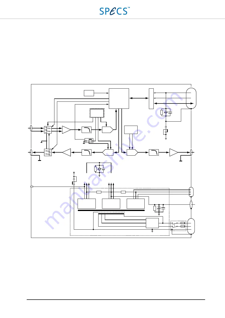
The block diagram of the SC5 is shown in the picture below.
Figure 1: Block diagram of the SC5. Only one analog input and one analog output are shown for clarity.
The SC5 can be divided into the following functional blocks: Analog inputs, analog outputs, fast analog output,
logic, and power supply.
Each analog input (AI) uses an instrumentation amplifier frontend, followed by a 5
th
order low-pass filter with a
corner frequency of 100 kHz (-3 dB), and then by an 18-bit 1 MS/s ADC. The ADC circuit uses the same
temperature-stabilized voltage reference as the analog outputs. For calibration purposes, the input signal can be
switched to GND, to the reference voltage, or to the corresponding analog output (AO1 to AI1, AO2 to AI2, …,
AO8 to AI8) for all inputs simultaneously. The electronic switch is controlled by software.
AI 1-8
AO 1-8
FAST AO
Fuses
AC
in
pu
t
PE
PE
Line filter
Power
switch
+5
V
D
G
N
D
-5
V
+1
5V
AG
N
D
-1
5V
+1
5V
A
U
X
G
N
D
-1
5V
Line
voltage
detection
G
N
D
B
N
C
co
nn
ec
to
r
A
U
X
PS
co
nn
ec
to
r
D
E
VI
C
E
S
C
01
/0
2/
03
co
nn
ec
to
r
±15V auxiliary
power supply
±15V
power supply
±5V
power supply
Power LED
Linear power supply
100
Ω
100
Ω
LPF
LPF
LPF
ADC
DAC
AGND
AGND
DAC
CPLD
Is
ol
at
io
n
1k
Ω
100n
FPGA DGND
FPGA +5V
Serial communication
PE
PE
PE
10k
Ω
100n
Temp.
sensor
FAST AO
Vref
Stabilized
Vref
AGND
AGND
U B
AGND
10k
Ω
1n
Summary of Contents for Nanonis SC5
Page 1: ...Signal Conversion SC5 User Manual November 2016 R6860...
Page 2: ......
Page 5: ...SC5 Signal Conversion Conventions 5...
Page 8: ......
Page 72: ......
Page 74: ......
Page 75: ...SC5 Signal Conversion Legal Information 75 Declaration of Conformity...


