background image


SC5 Signal Conversion 

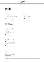
Index  

  77 

Index 

A


accuracy 31 

ambient temperature 43 

automatic line voltage selection 11, 15 

C


common-mode noise 25 

D


DAC glitch 31 

DEVICE RDIO cable 15 

differential buffer 25 

E


electrostatic discharge 28 

I


input gain 19 

input impedance 24, 40 

M


monotonicity 31 

N


Nanonis RC5 10, 13, 14, 15, 18 

O


output impedance 33, 35, 41, 42 

overcurrent detection 36, 37 

P


precision 31 

pulse-width modulation 31 

R


resolution 31, 33, 35, 41, 42 

S


shielded twisted-pair cable 19, 25 

slew rate 33, 35, 41, 42 

T


thermal fuse 36 

triaxial cable 19 

triboelectric effect 25 

W


wrist strap 28 


Summary of Contents for Nanonis SC5

Page 1: ...Signal Conversion SC5 User Manual November 2016 R6860...

Page 2: ......

Page 3: ...23 Specifications inputs 24 Analog Outputs 25 Analog outputs connection 25 Analog outputs schematic 28 Bipolar and unipolar operation 28 hrDAC 31 Introduction 31 Calibration procedure 32 Specificatio...

Page 4: ...Frequency response 51 Linearity 51 Harmonic distortion 52 Crosstalk 53 Analog outputs noise performance measurements 54 Spectral noise 54 Noise 0 1 Hz 10 Hz 55 Noise 10 Hz 300 kHz 56 Analog outputs DC...

Page 5: ...SC5 Signal Conversion Conventions 5...

Page 6: ...Hot surface Indicates that the surface of the instrument might become hot Avoid coming into contact with the hot surface Static sensitive devices Observe precautions for handling electrostatic sensiti...

Page 7: ...irements Do not install substitute parts or perform modifications to this instrument No user serviceable parts inside Do not operate the SC5 if it is damaged or not functioning properly Never use dama...

Page 8: ......

Page 9: ...f the instrument and explains its installation and operation This manual is not a service manual for the SC5 Revision history November 2016 R6860 Updated release of the SC5 manual Updated conformity d...

Page 10: ...s a custom temperature stabilized and thermally and mechanically isolated precision voltage reference Each function group has its own low noise voltage regulators and crosstalk is minimized further by...

Page 11: ...temperature stabilized voltage reference as the analog outputs For calibration purposes the input signal can be switched to GND to the reference voltage or to the corresponding analog output AO1 to AI...

Page 12: ...r jumpers of the outputs and the temperature inside the instrument A clock cleaning circuit provides a clean low jitter reference clock for the digital section and the AD DA converters The SC5 linear...

Page 13: ...f the external device connected to the auxiliary power supply connector 9 is drawing too much current more than 300 mA per rail the LED of the overloaded rail will start flashing with a frequency of 5...

Page 14: ...his guide It will be assumed that the SC5 is controlled using a Nanonis RC5 Please read the RC5 manual carefully before proceeding Content of delivery When first unpacking the SC5 please check for the...

Page 15: ...se only the provided power cord or power cords conforming to IEC60227 with a connector conforming to IEC60320 Connection to RC5 Only one single cable supplied with the SC5 is needed as a connection be...

Page 16: ...erwise the connectors might be damaged Do not overtighten the screws Note If a single SC5 is connected to the RC5 it must be connected to the SC 01 port at the back of the RC5 Do not connect it to the...

Page 17: ...GND and are not floated with respect to each other If the experimental setup requires AGND and PE to not be connected together the GND BNC connector 7 on the rear panel of the SC5 should be left open...

Page 18: ...on Figure 7 Powering of the SC5 Left side Location of the power switch at the back of the SC5 Right side LED which will turn on after powering the unit The SC5 is now ready for use Should the SC5 not...

Page 19: ...voltage with respect to AGND must never exceed 13 V or damage to the instrument will occur The limit is valid for both center pin and shield of the BNC connectors There are no external controls for t...

Page 20: ...d twisted pair cables can be used if the signal source is single ended but is referenced to a different GND than PE The GND can be on the shield of the connector which must then be isolated from PE or...

Page 21: ...mber of paired inputs is user selectable but only nearby inputs should be paired and only if at least one of the inputs is not assigned to a specific function by the software as default A typical conn...

Page 22: ...en the connectors shields in the experiment are connected to PE the following connection scheme should be used If the shields are separated from PE in the experiment the following wiring configuration...

Page 23: ...sses a 5th order Butterworth active low pass filter with a corner frequency of 100 kHz 3 dB before being digitized at a rate of 1 MS s with an 18 bit ADC Each input channel is completely independent f...

Page 24: ...bit 3 9 kS s 24 bit 240 S s DNL 1 LSB typical 18 bit INL 2 LSB typical 18 bit Analog input noise density 23 nV sqrt Hz 100 Hz Input range 10 V Gain 1 Converter noise density 650 nV sqrt Hz 10 Hz 230 n...

Page 25: ...controls for the analog outputs The output relays see the Analog outputs schematic section for details are controlled by software during the calibration procedure The outputs are configured for bipola...

Page 26: ...of the experiment or just the return path for the applied signal Shielded twisted pair cables should be used if there is a differential buffer after the input connector at the experiment as shown bel...

Page 27: ...connected to PE the following connection scheme should be used If the shields are separated from PE the following wiring configuration should be used The following configuration should be used if a s...

Page 28: ...to the experiment will also guarantee that line frequency components picked up from the cabling between SC5 and experiment can be filtered effectively For purely capacitive loads optimum frequency re...

Page 29: ...modification Before proceeding with the change of jumper positions please make sure that All analog inputs 2 and analog outputs 3 including the fast analog output 10 are disconnected from the experim...

Page 30: ...removal of the top cover an additional internal shield has to be removed The shield covers the entire analog output section and is located as indicated in the figure below Remove the three Phillips sc...

Page 31: ...nected to the top cover and to the rear panel before closing the instrument A loose grounding wire will impair safety of the instrument Also make sure that no shields screws tools or other objects hav...

Page 32: ...ut off at 41 67 kHz which is very close to the filter cut off meaning that a hrDAC generated frequency component will be visible at the output 24 bit resolution requires an even lower cut off of 20 83...

Page 33: ...ion DNL 0 5 LSB bipolar typical 0 75 LSB unipolar typical 20 bit INL 2 LSB typical 20 bit Output noise density 23 nV sqrt Hz 100 Hz 10 V output range RMS noise 0 1 10 Hz 180 nV rms 10 V output range P...

Page 34: ...ut is 10 V no unipolar setting and hrDAC cannot be used with this output This chapter explains how to connect the SC5 fast analog output FAST AO 10 to other equipment and explains in more detail the o...

Page 35: ...to load resistance 10 on 500 1 on 5 k 0 1 on 50 k Output impedance 50 short circuit safe Analog bandwidth DC 1 1 MHz 3 dB Analog filter type 1st order DA converter 20 bit monotonic 1 MS s Effective re...

Page 36: ...vercurrent by a current detection circuit which disables the output when the connected instrument draws more than 300 mA per supply rail In that case the status LED 8 of the overloaded rail will start...

Page 37: ...ption from the auxiliary power supply will increase the temperature of the SC5 due to additional thermal dissipation of the power supply Make sure that the SC5 is operated within the specified tempera...

Page 38: ...assignment of the auxiliary power supply receptacle Note that the casing of the receptacle is connected to PE in contrast to the Nanonis SC4 and OC4 where the casing is connected to AUX power supply G...

Page 39: ...ved REASON The external device is drawing too much current SOLUTION Check for a short circuit as above If there is no short circuit the external device is drawing more than 300 mA per rail from the SC...

Page 40: ...rential input impedance 2 M DC Analog bandwidth DC 100 kHz 3 dB Analog filter type 5th order Butterworth Gain 1 AD converter 18 bit no missing codes 1 MS s Effective resolution 20 bit 62 5 kS s 22 bit...

Page 41: ...sation DNL 0 5 LSB bipolar typical 0 75 LSB unipolar typical 20 bit INL 2 LSB typical 20 bit Output noise density 23 nV sqrt Hz 100 Hz 10 V output range RMS noise 0 1 10 Hz 180 nV rms 10 V output rang...

Page 42: ...noise 0 1 10 Hz 600 nV rms 10 V output range Peak peak noise 0 1 10 Hz 2 5 Vp p 10 V output range RMS noise 10 Hz 300 kHz 12 V rms 10 V output range Peak peak noise 10 Hz 300 kHz 105 Vp p 10 V output...

Page 43: ...condensing in accordance with IEC 60068 2 56 Maximum altitude 2000 m Pollution degree 2 indoor use only Installation category II Mains supply voltage fluctuations Are not to exceed 10 of nominal supp...

Page 44: ...22 Spectral noise of the analog inputs up to a frequency of 1 kHz Figure 23 Spectral noise of the analog inputs showing the full sampling range left and the low frequency range below 60 Hz right The a...

Page 45: ...000 10 Hz 620 100 Hz 220 1 kHz 155 10 kHz 140 50 kHz 140 100 kHz 145 Table 2 Spectral noise density for different frequencies Noise and oversampling The input noise voltage of the analog inputs is mea...

Page 46: ...ge mV 0 5 0 4 0 3 0 2 0 1 0 0 1 0 2 0 3 0 4 0 5 Input range 10 V Oversampling 1x 0 10 20 30 40 50 60 Time ms Input noise voltage V Input range 10 V Oversampling 32x 80 60 40 20 0 20 40 60 80 0 10 20 3...

Page 47: ...21 62 4096x 0 12 Hz 122 Hz 41 6 2 21 62 8192x 0 06 Hz 61 Hz 41 6 2 21 62 16384x 0 03 Hz 30 5 Hz 41 6 2 21 62 32768x 0 015 Hz 15 3 Hz 40 6 4 21 58 Table 3 Input noise voltage and effective resolution a...

Page 48: ...gain error The offset of the SC5 inputs is measured with the SC5 inputs connected to GND The maximum absolute offset and the maximum relative offset between channels for uncalibrated and calibrated in...

Page 49: ...eading 7 mV 7 mV 30 mV Yes 0 76 of reading 25 V 25 V 7 6 mV Table 6 Accuracy of the analog inputs Input stability and temperature dependence 12 hour stability The stability of the input voltage is mea...

Page 50: ...erably less than the external temperature meaning that the temperature coefficient is smaller when based on the environment temperature Note During normal operation the SC5 reaches a typical operating...

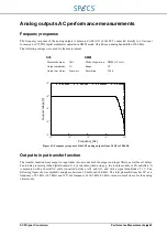
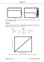
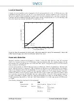
Page 51: ...z to 500 kHz Linearity Linearity is measured by applying a 100 Hz sinewave with amplitudes ranging from 10 V 0 dBFS to 100 V 100 dBFS generated by AO1 to AI1 The amplitude was calibrated each time usi...

Page 52: ...hout using voltage dividers Note that harmonic distortion measurements also include harmonic distortion of the output signal of the SC5 and the waveform generator meaning that the numbers are a lower...

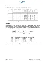
Page 53: ...Output range 10 V Frequency Crosstalk amplitude FFT resolution 100 Hz 600 nV Hz 50 mHz 1 kHz 600 nV Hz 0 5 Hz 10 kHz 600 nV Hz 5 Hz 100 kHz 750 nV Hz 50 Hz Table 9 Crosstalk signal amplitude of the an...

Page 54: ...age frequency and harmonic components strongly depend on the measurement set up The following settings have been used for the measurement SC5 DMM Measured output AO1 Mode of operation Digitizer DC vol...

Page 55: ...line frequency 50 Hz and its second and third harmonic as well as sampling frequency Values in brackets are measured using the SC5 inputs which is a measurement set up less susceptible to hum pick up...

Page 56: ...Hz 300 kHz The noise of the SC5 outputs above 10 Hz is measured with the same set up as described in the previous section The upper frequency limit is given by the analog bandwidth of the multimeter T...

Page 57: ...e output noise above 0 1 Hz for different cut off frequencies is listed in the table below for first and second order active filters built in filters of the SR560 preamplifier The sampling frequency o...

Page 58: ...the INL would show a lower INL than in themeasurement below The following settings have been used for the measurement SC5 DMM Measured output AO1 Mode of operation DMM DC volts Range 10 V Resolution...

Page 59: ...n in the table below The following settings have been used for the measurement SC5 DMM Measured output AO1 Mode of operation DMM DC volts Output amplitude 0 V 10 V Range 100 mV and 10 V Resolution 26...

Page 60: ...ion The measurement was done with AO1 connected to a National Instruments 4071 PXI digital multimeter operated in digitizer mode 6 5 digits at 100 S s The following settings have been used for the mea...

Page 61: ...drift reflects changes of the internal temperature of the SC5 with an increase in temperature leading to a slight decrease of the output voltage The DMM has a temperature coefficient of 0 3 ppm of re...

Page 62: ...ronment temperature Note During normal operation the SC5 reaches a typical operating temperature of 38 42 C The temperature coefficient around the operating temperature is lower than the worst case va...

Page 63: ...se of the SC5 analog outputs from 10 Hz to 100 kHz Output to input transfer function The transfer function from output to input takes into account both the output and input filters as well as all dela...

Page 64: ...f 100 Hz and amplitudes ranging from 10 V 0 dBFS to 10 V 120 dBFS The following settings were used for the measurement SC5 DMM Measured output AO1 Mode of operation Digitizer AC volts Output signal Si...

Page 65: ...10 the signal frequency for 10 kHz The FFT has a resolution of 100 000 points The measured quantities are SINAD SIgnal to Noise And Distortion THD N Total Harmonic Distortion plus Noise both measured...

Page 66: ...easurements for a 90 mV signal at 100 Hz left 1 kHz center and 10 kHz right 0 100 200 300 400 500 600 700 800 900 Frequency Hz Output dBFS 20 0 20 40 60 80 100 120 140 160 0 1 2 3 4 5 6 7 8 9 10 Frequ...

Page 67: ...tanford Research Systems SR560 low noise differential preamplifier set to gain 1000 and to a National Instruments 4071 PXI digital multimeter operated in digitizer mode for recording the spectrum whil...

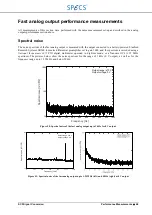
Page 68: ...ing a National Instruments 4071 PXI digital multimeter operated in digitizer mode or a Nanonis OC4 1 25 MHz spectrum The pictures below show the noise spectrum for the range of 1 kHz 0 V output as wel...

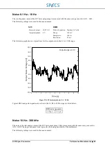
Page 69: ...ace for the output noise in the 0 1 to 10 Hz range Figure 52 SC5 fast output noise 0 1 10 Hz Typical RMS and peak to peak noise values in the 0 1 Hz to 10 Hz range are listed below RMS noise p p noise...

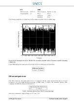
Page 70: ...s in the 10 Hz to 300 kHz range are listed below RMS noise p p noise 12 V 105 V Offset and gain error The offset of the SC5 fast output when set to 0 V is measured with the output connected directly t...

Page 71: ...esponse shows the effect of undersampling and is therefore not the frequency response of the analog output stage Specifications of the output stage are 0 8 dB at 500 kHz and 2 7 dB at 1 MHz The follow...

Page 72: ......

Page 73: ...tion against SPECS must be brought within one year after the cause of action accrues SPECS shall not be liable for any delay in performance due to causes beyond its reasonable control The warranty pro...

Page 74: ......

Page 75: ...SC5 Signal Conversion Legal Information 75 Declaration of Conformity...

Page 76: ...SC5 Signal Conversion Legal Information 76...

Page 77: ...buffer 25 E electrostatic discharge 28 I input gain 19 input impedance 24 40 M monotonicity 31 N Nanonis RC5 10 13 14 15 18 O output impedance 33 35 41 42 overcurrent detection 36 37 P precision 31 pu...

Page 78: ...SC5 Signal Conversion Index 78 SPECS Surface Nano Analysis GmbH Voltastrasse 5 13355 Berlin Germany Tel 49 30 46 78 24 0 Fax 49 30 46 42 083 Email support specs com Web www specs com...

Reviews: