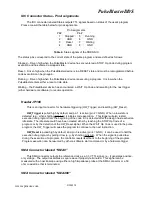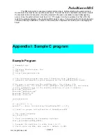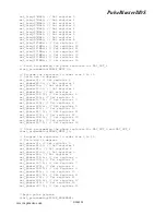
PulseBlasterDDS
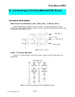
Board Architecture
Block Diagram
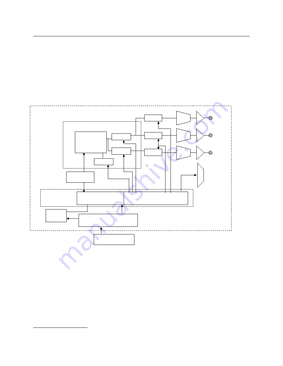
Figure 2 presents the general architecture of the PulseBlasterDDS system. The two major building
blocks are the DDS Core and the Pulse Programming and Timing Processor Core (PP Core). The
DDS Core contains a numerically controlled oscillator and has 16 programmable frequency registers
that are under the pulse program control. Prior to gating, the DDS signal can be phase offset by one of
two sets of 16 programmable phase registers. The PP Core controls the timing of the gating pulses
and provides the necessary control signals for frequency and phase registers. The DDS and PP cores
have been integrated onto a single silicon chip. High performance DAC chips and high current output
amplifiers complement the design. User control to the system is provided through the host-
programming interface over the PCI bus.
Figure 2:
PulseBlasterDDS board architecture
Output signals
The PulseBlasterDDS comes with three analog output channels configured to output radio-frequency
(RF/IF) pulses, and 10 digital output signal lines (one of the output lines has a dual use and
functions as a phase reset for the DDS generator). The frequency and phase of the RF pulses generated
by the DDS are under the control of the user and are specified through software programming. The phase
of the numerically controlled oscillator can be reset on demand within the pulse program.
PulseBlasterDDS provides the ability to gate the output of the DDS channels allowing for independent
pulsed RF operation. With digital sampling rate of 100 MHz (max. reference clock frequency), the
maximum theoretical output frequency is 50 MHz (the Nyquist Theorem).
1
The analog output signal is
available on an on-board SMA connector. The output impedance of the analog signal is 50-ohms. There
are no interpolating filters on board.
1
Note that the usefulness of a waveform with two samples per period is limited, and, depending on applications,
practical considerations would often call for more than two samples per period.
9/20/20056
DAC
RF
Outputs
(SMA)
Phase0-15
Gate
Numerically
Conrolled
Oscillator
DAC
Gate
Phase0-15
Freq0-15
Reference Clock
Oscillator
Precision Timing Processor
Output and Control Register
TTL
Outputs
(DB-25)
SRAM
Host Programming Interface
User Control
PulseBlasterDDS-III
© 2004 SpinCore Technologies, Inc.
http://www.spincore.com
Gate
DAC
DDS Core
Pulse Timing
Core
Tx
Rx
www.spincore.com


