background image

L6470

Phase current control

Doc ID 16737 Rev 2

33/64


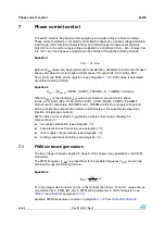
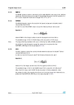
Motor supply voltage compensation can be enabled setting high the EN_VSCOMP bit of the 
CONFIG register (see 

Table 21

, paragraph 

9.1.21

). If EN_VSCOMP bit is low the 

compensation is disabled and the internal analog to digital converter is at user disposal; 
sampling rate is always equal to PWM frequency.

7.6 Winding 

resistance 

thermal drift compensation

The higher is the winding resistance the greater is the voltage to be applied in order to 
obtain the same phase current.

The L6470 integrates a register (K_THERM) which can be used to compensate phase 
resistance increment due by temperature rising.

The value in K_THERM register (see paragrap

9.1.15

) multiplies duty cycle value allowing 

to face higher phase resistance value.

The compensation algorithm and the eventual motor temperature measurement should be 
implemented by microcontroller firmware.

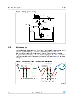
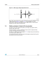
Figure 15.

Motor supply voltage compensation circuit


!-V

!$#).

!$#

F

07-

!$#?/54

6

3

6

2%'

2

!

2

"

6

!$#).

6

3

X2

"

2

!

2

"


Summary of Contents for L6470H

Page 1: ...RDSon DMOS full bridge with all of the power switches equipped with an accurate on chip current sensing circuitry suitable for non dissipative current control and overcurrent protections Thanks to a unique control system a true 1 128 steps resolution is achieved The digital control core can generate user defined motion profiles with acceleration deceleration speed or target position easily program...

Page 2: ... pump 19 6 4 Microstepping 20 6 5 Absolute position counter 21 6 6 Programmable speed profiles 21 6 6 1 Infinite acceleration deceleration mode 21 6 7 Motor control commands 22 6 7 1 Constant speed commands 22 6 7 2 Positioning commands 22 6 7 3 Motion commands 23 6 7 4 Stop commands 23 6 7 5 Step clock mode 24 6 8 Internal oscillator and oscillator driver 24 6 8 1 Internal oscillator 24 6 8 2 Ext...

Page 3: ...7 1 PWM sinewave generators 30 7 2 Sensorless stall detection 31 7 3 Low speed optimization 31 7 4 BEMF compensation 32 7 5 Motor supply voltage compensation 32 7 6 Winding resistance thermal drift compensation 33 8 Serial interface 34 9 Programming manual 36 9 1 Registers and flags description 36 9 1 1 ABS_POS 37 9 1 2 EL_POS 37 9 1 3 MARK 38 9 1 4 SPEED 38 9 1 5 ACC 38 9 1 6 DEC 39 9 1 7 MAX_SPE...

Page 4: ...9 2 3 SetParam PARAM VALUE 54 9 2 4 GetParam PARAM 54 9 2 5 Run DIR SPD 55 9 2 6 StepClock DIR 55 9 2 7 Move DIR N_STEP 56 9 2 8 GoTo ABS_POS 56 9 2 9 GoTo_DIR DIR ABS_POS 57 9 2 10 GoUntil ACT DIR SPD 57 9 2 11 ReleaseSW ACT DIR 58 9 2 12 GoHome 58 9 2 13 GoMark 58 9 2 14 ResetPos 59 9 2 15 ResetDevice 59 9 2 16 SoftStop 59 9 2 17 HardStop 59 9 2 18 SoftHiZ 60 9 2 19 HardHiZ 60 9 2 20 GetStatus 6...

Page 5: ...hard stop interrupt mode 46 Table 24 Overcurrent event 47 Table 25 Programmable power bridge output slew rate values 47 Table 26 Motor supply voltage compensation enable 47 Table 27 PWM frequency integer division factor 47 Table 28 PWM frequency multiplication factor 48 Table 29 Available PWM frequencies kHz 8 MHz oscillator frequency 48 Table 30 Available PWM frequencies kHz 16 MHz oscillator fre...

Page 6: ...etDevice command structure 59 Table 51 SoftStop command structure 59 Table 52 HardStop command structure 59 Table 53 SoftHiZ command structure 60 Table 54 HardHiZ command structure 60 Table 55 GetStatus command structure 60 Table 56 HTSSOP28 mechanical data 61 Table 57 Document revision history 63 ...

Page 7: ...2 Figure 8 Positioning command examples 23 Figure 9 Motion commands examples 23 Figure 10 OSCIN and OSCOUT pins configurations 25 Figure 11 External switch connection 27 Figure 12 Internal 3 V linear regulator 28 Figure 13 Current distortion and compensation 31 Figure 14 BEMF compensation curve 32 Figure 15 Motor supply voltage compensation circuit 33 Figure 16 SPI timings diagram 34 Figure 17 Dai...

Page 8: ...pump VDD SPI Registers Control Logic Current DACs Comparators Temperature sensing Current sensing STBY RST FLAG CS CK SDO SDI BUSY SYNC SW STCK DGND VDD OSCIN OSCOUT ADCIN VREG CP VBOOT AGND PGND PGND VSA VSA OUT1A OUT2A VSB VSB OUT1B OUT2B HS A1 LS A1 HS A2 LS A2 HS B1 LS B1 HS B2 LS B2 HS A1 LS A1 HS A2 LS A2 HS B1 LS B1 HS B2 LS B2 VDD Vboot Vboot Vboot Vboot ...

Page 9: ...ial voltage between VSA OUT1A OUT2A PGND and VSB OUT1B OUT2B PGND pins VSA VSB VS 48 V VLOGIC Logic inputs voltage range 0 3 to 5 5 V Iout 1 1 Maximum output current limit is related to metal connection and bonding characteristics Actual limit must satisfy maximum thermal dissipation constraints R m s output current 3 A Iout_peak 1 Pulsed output current TPULSE 1 ms 7 A TOP Operating junction tempe...

Page 10: ...ce supply voltage 3 3 V logic outputs 3 3 V 5 V logic outputs 5 VS Motor supply voltage VSA VSB VS 8 45 V Vout_diff Differential voltage between VSA OUT1A OUT2A PGND and VSB OUT1B OUT2B PGND pins VSA VSB VS 45 V VREG in Logic supply voltage VREG voltage imposed by external source 3 2 3 3 V VADC Integrated ADC input voltage ADCIN pin 0 VREG V Tj Operating junction temperature 25 125 C ...

Page 11: ... 65 mA Tj WRN Thermal warning temperature 130 C Tj SD Thermal shutdown temperature 160 C Charge pump Vpump Voltage swing for charge pump oscillator 10 V fpump min Minimum charge pump oscillator frequency 1 660 kHz fpump max Maximum charge pump oscillator frequency 1 800 kHz Iboot Average boot current fsw A fsw B 15 6 kHz POW_SR 10 1 1 1 4 mA Output DMOS transistor RDS on High side switch ON resist...

Page 12: ...0 POW_SR 10 Iout 1A 110 POW_SR 01 Iout 1A 75 Dead time and blanking tDT Dead time POW_SR 00 250 ns POW_SR 11 fOSC 16MHz 375 POW_SR 10 fOSC 16MHz 625 POW_SR 01 fOSC 16MHz 875 tblank Blanking time POW_SR 00 250 ns POW_SR 11 fOSC 16MHz 375 POW_SR 10 fOSC 16MHz 625 POW_SR 01 fOSC 16MHz 875 Source drain diodes VSD HS High side diode forward ON voltage Iout 1 A 1 1 1 V VSD LS Low side diode forward ON v...

Page 13: ...ternally supplied 2 2 5 µA fSTCK Step clock input frequency 2 MHz Internal oscillator and external oscillator driver fosc i Internal oscillator frequency Tj 25 C VREG 3 3 V 3 16 3 MHz fosc e Programmable external oscillator frequency 8 32 MHz VOSCOUTH OSCOUT clock source high level voltage Internal oscillator 3 3 V VREG externally supplied IOSCOUT 4 mA 2 4 V VOSCOUTL OSCOUT clock source low level ...

Page 14: ... fosc 32MHz 5 6 125 NPWM PWM resolution 8 bit Overcurrent protection OCD_thMAX Maximum programmable overcurrent detection threshold OCD_TH 1111 6 A OCD_thMIN Minimum programmable overcurrent detection threshold OCD_TH 0000 0 375 A OCD_thRES Programmable overcurrent detection threshold resolution 0 375 A tOCD Flag OCD to Flag signal delay time dIout dt 350A µs RFLAG TBD 650 1000 ns tOCD SD OCD to s...

Page 15: ...nalog to digital converter reference voltage VREG V fS Analog to digital converter sampling frequency fPWM kHz 1 Accuracy depends on oscillator frequency accuracy 2 Tested at 25 C in a restricted range and guaranteed by characterization 3 Rise and fall time depends on motor supply voltage value Refer to SRout values in order to evaluate the actual rise and fall time 4 Not valid for STBY RST pin wh...

Page 16: ...tor pin 1 To connect an external oscillator or clock source If this pin is UNUSED it should be connected to ground 8 OSCOUT Analog output Oscillator pin 2 To connect an external oscillator When the internal oscillator is used this pin can supply a 2 4 8 16 MHz If this pin is UNUSED it should be left floating 10 CP Output Charge pump oscillator output 11 VBOOT Supply voltage Bootstrap voltage neede...

Page 17: ...n can be configured to generate a synchronization signal 18 SDO Logic output Data output pin for serial interface 20 SDI Logic input Data input pin for serial interface 19 CK Logic input Serial interface clock 23 CS Logic input Chip Select input pin for serial interface 24 FLAG Open drain output Status Flag pin An internal open drain transistor can pull the pin to GND when a programmed alarm condi...

Page 18: ...ipolar stepper motor control application using L6470 Table 6 Typical application values Name value CVS 220 nF CVSPOL 100 µF CREG 100 nF CREGPOL 47 µF CDD 100 nF CDDPOL 10 µF D1 BAT46SW or 2x 1N4148 CBOOT 220 nF CFLY 10 nF RPU 39 kΩ RSW 100 Ω CSW 10 nF RA 2 7 kΩ VS 36 V RB 62 kΩ VS 36 V ...

Page 19: ...top included 6 2 Logic I O Pins CS CK SDI STCK SW and STBY RST are TTL CMOS 3 3V 5V compatible logic inputs Pin SDO is a TTL CMOS compatible logic output VDD pin voltage sets the logic output pin voltage range when it is connected to VREG or 3 3V external supply voltage the output is 3 3V compatible When VDD is connected to a 5V supply voltage SDO is 5V compatible VDD is not internally connected t...

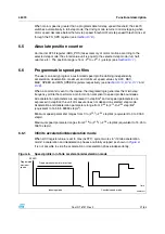
Page 20: ...tep mode is changed the electrical position i e the point of microstepping sinewave that is generated is reset to first microstep and the absolute position counter value see Section 6 5 becomes meaningless Figure 5 Normal mode and microstepping 128 microsteps V 63 63 6 0 6 6 6 0 F05 0 TO HIGH SIDE GATE DRIVERS 63 6 0 6 4 9 6 4 0 6 V STEP STEP STEP STEP STEP STEP 2ESET POSITION STEP STEP STEP STEP ...

Page 21: ...hen a command is sent to the device the integrated logic generates the microstep frequency profile that performs a motor motion compliant to speed profile boundaries All acceleration parameters are expressed in step tick2 and all speed parameters are expressed in step tick the unit of measure does not depend on selected step mode Acceleration and deceleration parameters range from 2 40 to 212 2 2 ...

Page 22: ...leration deceleration value set in ACC and DEC registers A new constant speed command can be requested anytime Figure 7 Constant speed commands examples 6 7 2 Positioning commands An absolute positioning command produces a motion in order to reach a user defined position that is sent to the device together with the command The position can be reached performing the minimum path minimum physical di...

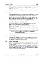
Page 23: ...otor to stop Stop commands can be sent anytime SoftStop command causes the motor to decelerate with programmed deceleration value until MIN_SPEED value is reached and then stops the motor keeping the rotor position a holding torque is applied HardStop command stops the motor instantly ignoring deceleration constrain and keeping the rotor position a holding torque is applied V ORWARD DIRECTION 0RES...

Page 24: ...nal oscillator crystal or ceramic resonator or a direct clock signal These working modes can be selected by EXT_CLK and OSC_SEL parameters in the CONFIG register see Table 22 At power up the device starts using the internal oscillator and provides a 2 MHz clock signal on the OSCOUT pin Attention In any case before changing clock source configuration a hardware reset is mandatory 6 8 1 Internal osc...

Page 25: ...ent is expired and a GetStatus command is sent to the IC see paragraphs 9 1 22 and 9 1 17 Overcurrent event expires when all the power MOSFET currents fall below the programmed overcurrent threshold Table 7 CL values according to external oscillator frequency Crystal resonator freq 1 1 First harmonic resonance frequency CL 2 2 Lower ESR value allows driving greater load capacitors 8MHz 25pF ESRmax...

Page 26: ... forced low see paragraph 9 1 22 until the temperature decrease below Tj WRN and a GetStatus command is sent to the IC see paragraphs 9 1 22 and 9 2 20 When the thermal shutdown threshold Tj OFF is reached the device goes in thermal shutdown condition the TH_SD bit in the STATUS register is forced low the power bridges are disabled bridges in high impedance state and the HiZ bit in the STATUS regi...

Page 27: ...US register indicates if the switch is open 0 or closed 1 see paragraph 9 1 22 the bit value is refreshed at every system clock cycle 125 ns SW_EVN flag of STATUS register is raised when a switch turn on event SW input falling edge is detected see paragraph 9 1 22 A GetStatus command releases the SW_EVN flag see paragraph 9 2 20 By default a switch turn on event causes a HardStop interrupt SW_MODE...

Page 28: ...supply VSA and VSB In order to make the voltage regulator stable at least 22 µF should be connected between VREG pin and ground suggested value is 47 µF The internal voltage regulator can be used to supply the VDD pin in order to make the device digital output range 3 3 V compatible Figure 12 A digital output range 5 V compatible can be obtained connecting VDD pin to an external 5 V voltage source...

Page 29: ...works as synchronization signal when SYNC_EN bit is set high In this mode a step clock signal is provided on output according to SYNC_SEL and STEP_SEL parameters combination see paragraph 9 1 19 6 18 FLAG pin By default an internal open drain transistor pulls the FLAG pin to ground when at least one of the following conditions occurs Power up or standby reset exit Stall detection on A bridge Stall...

Page 30: ..._COMP is the BEMF compensation curve value VSCOMP and K_THERM are the motor supply voltage and winding resistance compensation factors and microstep is the current microstep value fraction of target peak current L6470 offers various methods to guarantee a stable current value allowing the compensation of low speed optimization see paragraph 7 3 back electromotive force value see paragraph 7 4 moto...

Page 31: ... voltage the resulting phase current can be distorted As a consequence the motor position is different from the ideal one see Figure 13 L6470 implements a low speed optimization in order to remove this effect Figure 13 Current distortion and compensation The optimization can be enabled setting high the LSPD_OPT bit in MIN_SPEED register see paragraph 9 1 8 and is active into speed range from zero ...

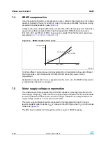
Page 32: ...and consequently two different compensation curves can be programmed Acceleration compensation curve is applied when the motor runs No BEMF compensation is applied when the motor is stopped 7 5 Motor supply voltage compensation The sinewave amplitude generated by the PWM modulators is directly proportional to the motor supply voltage VS When the motor supply voltage is different from its nominal v...

Page 33: ...ompensation The higher is the winding resistance the greater is the voltage to be applied in order to obtain the same phase current The L6470 integrates a register K_THERM which can be used to compensate phase resistance increment due by temperature rising The value in K_THERM register see paragraph 9 1 15 multiplies duty cycle value allowing to face higher phase resistance value The compensation ...

Page 34: ...t significant bit first The SDI is sampled on the rising edges of the CK All output data bytes are shifted out of the device through the SDO output most significant bit first The SDO is latched on the falling edges of the CK When a return value from the device is not available an all zero byte is sent After each byte transmission the CS input must be raised and be kept high for at least tdisCS in ...

Page 35: ...L6470 Serial interface Doc ID 16737 Rev 2 35 64 Figure 17 Daisy chain configuration V 34 34 30 SIGNALS 6 3 3 3 3 3 3 3 3 3 6 3 3 3 6 3 3 3 YTE YTE YTE YTE YTE YTE YTE YTE ...

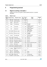
Page 36: ... 991 8 step s R WR h08 MIN_SPEED Minimum speed 13 000 0 step tick 0 step s R WS h15 FS_SPD Full step speed 10 027 150 7e 6 step tick 602 7 step s R WR h09 KVAL_HOLD Holding KVAL 8 29 0 16 VS R WR h0A KVAL_RUN Constant speed KVAL 8 29 0 16 VS R WR h0B KVAL_ACC Acceleration starting KVAL 8 29 0 16 VS R WR h0C KVAL_DEC Deceleration starting KVAL 8 29 0 16 VS R WR h0D INT_SPD Intersect speed 14 0408 6...

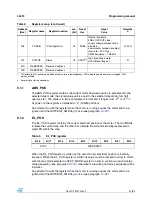
Page 37: ...s written its value must be masked in order to match with the step mode selected in STEP_MODE register in order to avoid a wrong microstep value generation see paragraph 9 1 19 otherwise the resulting microstep sequence will be incorrect Any attempt to write the register when the motor is running causes the command to be ignored and the NOTPERF_CMD flag to rise see paragraph 9 1 22 h18 CONFIG IC c...

Page 38: ... step s Note The range effectively available to the user is limited by the MAX_SPEED parameter Any attempt to write the register causes the command to be ignored and the NOTPERF_CMD flag to rise see paragraph 9 1 22 9 1 5 ACC The ACC register contains the speed profile acceleration expressed in step tick2 format unsigned fixed point 0 40 In order to convert ACC value in step s2 the following formu...

Page 39: ...graph 9 1 22 9 1 7 MAX_SPEED The MAX_SPEED register contains the speed profile maximum speed expressed in step tick format unsigned fixed point 0 18 In order to convert it in step s the following formula can be used Equation 7 where MAX_SPEED is the integer number stored into the register and tick is 250 ns The available range is from 15 25 to 15610 step s with a resolution of 15 25 step s 9 1 8 M...

Page 40: ... always works in microstepping mode SPEED must go beyond the threshold to switch to full step mode Setting FS_SPD to zero has not the same effect as setting step mode to full step two phase on zero FS_SPD value is equivalent to a speed threshold of about 7 63 step s The available range is from 7 63 to 15625 step s with a resolution of 15 25 step s 9 1 10 KVAL_HOLD KVAL_RUN KVAL_ACC and KVAL_DEC Th...

Page 41: ...om 0 to 0 004 with a resolution of 0 000015 When ST_SLP FN_SLP_ACC and FN_SLP_DEC parameters are set to zero no BEMF compensation is performed Any attempt to write the register when the motor is running causes the command to be ignored and the NOTPERF_CMD flag to rise see paragraph 9 1 22 9 1 13 FN_SLP_ACC The FN_SLP_ACC register contains the BEMF compensation curve slope that is used when the spe...

Page 42: ...mpensation system see paragraph 7 6 The available range is from 1 to 1 46875 with a resolution of 0 03125 as shown in Table 12 9 1 16 ADC_OUT The ADC_OUT register contains the result of the analog to digital conversion of the ADCIN pin voltage the result is available even if the supply voltage compensation is disabled Any attempt to write to the register causes the command to be ignored and the NO...

Page 43: ... mA to 4 A with a resolution of 31 25 mA 9 1 19 STEP_MODE The STEP_MODE register has the following structure The STEP_SEL parameter selects one of eight possible stepping modes Table 14 Overcurrent detection threshold OCD_TH 3 0 Overcurrent detection threshold 0 0 0 0 375 mA 0 0 0 1 750 mA 1 1 1 0 5 625 A 1 1 1 1 6 A Table 15 Stall detection threshold STALL_th 6 0 Stall detection threshold 0 0 0 0...

Page 44: ...se when SYNC_EN bit is set high BUSY SYNC output provides a clock signal according to SYNC_SEL parameter Table 17 Step mode selection STEP_SEL 2 0 Step mode 0 0 0 Full step 0 0 1 Half step 0 1 0 1 4 microstep 0 1 1 1 8 microstep 1 0 0 1 16 microstep 1 0 1 1 32 microstep 1 1 0 1 64 microstep 1 1 1 1 128 microstep Table 18 SYNC output frequency STEP_SEL fFS is the full step frequency 000 001 010 011...

Page 45: ...s the following structure Table 19 SYNC signal source SYNC_SEL 2 0 Source 0 0 0 EL_POS 7 0 0 1 EL_POS 6 0 1 0 EL_POS 5 0 1 1 EL_POS 4 1 0 0 EL_POS 3 1 0 1 EL_POS 2 1 1 0 EL_POS 1 1 1 1 EL_POS 0 Table 20 ALARM_EN register ALARM_EN bit Alarm condition 0 LSB Overcurrent 1 Thermal shutdown 2 Thermal warning 3 Under voltage 4 Stall detection Bridge A 5 Stall detection Bridge B 6 Switch turn on event 7 ...

Page 46: ...Crystal resonator driving 0 1 0 1 External crystal or resonator 16MHz Crystal reson ator driving Crystal resonator driving 0 1 1 0 External crystal or resonator 24MHz Crystal reson ator driving Crystal resonator driving 0 1 1 1 External crystal or resonator 32MHz Crystal reson ator driving Crystal resonator driving 1 1 0 0 Ext clock source 8MHz Crystal resonator driver disabled Clock source Suppli...

Page 47: ...uency generation Table 24 Overcurrent event OC_SD Overcurrent event 1 Bridges shut down 0 Bridges do not shut down Table 25 Programmable power bridge output slew rate values POW_SR 1 0 Output Slew rate 1 V µs 1 See SRout_r and SRout_f parameters in the electrical characteristics Table 4 for details 0 0 180 0 1 180 1 0 290 1 1 530 Table 26 Motor supply voltage compensation enable EN_VSCOMP Motor su...

Page 48: ...M frequency multiplication factor F_PWM_DEC 2 0 Multiplication factor 0 0 0 0 625 0 0 1 0 75 0 1 0 0 875 0 1 1 1 1 0 0 1 25 1 0 1 1 5 1 1 0 1 75 1 1 1 2 Table 29 Available PWM frequencies kHz 8 MHz oscillator frequency F_PWM_DEC F_PWM_ INT 000 001 010 011 100 101 110 111 000 9 8 11 7 13 7 15 6 19 5 23 4 27 3 31 3 001 4 9 5 9 6 8 7 8 9 8 11 7 13 7 15 6 010 3 3 3 9 4 6 5 2 6 5 7 8 9 1 10 4 011 2 4 2...

Page 49: ...3 7 15 6 100 3 9 4 7 5 5 6 3 7 8 9 4 10 9 12 5 101 3 3 3 9 4 6 5 2 6 5 7 8 9 1 10 4 110 2 8 3 3 3 9 4 5 5 6 6 7 7 8 8 9 Table 31 Available PWM frequencies kHz 24 MHz oscillator frequency F_PWM_DEC F_PWM_INT 000 001 010 011 100 101 110 111 000 29 3 35 2 41 0 46 9 58 6 70 3 82 0 93 8 001 14 6 17 6 20 5 23 4 29 3 35 2 41 0 46 9 010 9 8 11 7 13 7 15 6 19 5 23 4 27 3 31 3 011 7 3 8 8 10 3 11 7 14 6 17 ...

Page 50: ... respectively The NOTPERF_CMD and WRONG_CMD flags are active high and indicate respectively that the command received by SPI can t be performed or does not exist at all The SW_F report the SW input status low for open and high for closed The SW_EVN flag is active high and indicates a switch turn on event SW input falling edge Table 32 Available PWM frequencies kHz 32 MHz oscillator frequency F_PWM...

Page 51: ...high after the command have been completed The SCK_MOD bit is an active high flag indicating that the device is working in step clock mode In this case the step clock signal should be provided through STCK input pin The DIR bit indicates the current motor direction MOT_STATUS indicates the current motor status Any attempt to write to the register causes the command to be ignored and the NOTPERF_CM...

Page 52: ...R direction GoUntil ACT DIR SPD 100 0 ACT 01 DIR Perform a motion in DIR direction with speed SPD until SW is closed the ACT action is executed then a SoftStop takes place ReleseSW ACT DIR 100 1 ACT 01 DIR Performs a motion in DIR direction at minimum speed until the SW is released open the ACT action is executed then a HardStop takes place GoHome 011 1 0 00 0 Brings the motor in HOME position GoM...

Page 53: ...new commands can be sent If a command requiring a response is sent before the previous response is completed the response transmission is aborted and the new response is loaded into output communication buffer see Figure 20 Figure 20 Command response aborted When a byte that does not correspond to a command is sent to the IC it is ignored and the WRONG_CMD flag in STATUS register is raised see par...

Page 54: ... value causes the command to be ignored and WRONG_CMD flag to rise at the end of command byte as like as unknown command code is sent 9 2 4 GetParam PARAM This command reads the current PARAM register value PARAM is the respective register address listed in Table 11 All registers can be read anytime Returned value is the register one at the moment of SetParam command decoding If register values ch...

Page 55: ...5 and 9 1 22 Device exits from step clock mode when a constant speed absolute positioning or motion command is sent through SPI Motion direction is imposed by the respective StepClock command argument and can by changed by a new StepClock command without exiting the step clock mode Events that cause bridges to be forced in high impedance state overtemperature overcurrent etc do not cause the devic...

Page 56: ... produces a motion to ABS_POS absolute position through the shortest path The ABS_POS value is always in agreement with the selected step mode the parameter value unit is equal to the selected step mode full half quarter etc This command can be given when the outputs are in high impedance or the motor is stopped or running with constant speed Any attempt to perform a GoTo command when a previous c...

Page 57: ...the ABS_POS register is reset if ACT 0 or the ABS_POS register value is copied into the MARK register if ACT 1 then the system performs a SoftStop command The SPD value is expressed in step tick format unsigned fixed point 0 28 that is the same format that SPEED register see paragraph 9 1 4 SPD value should be lower than MAX_SPEED and greater than MIN_SPEED otherwise the target speed will be impos...

Page 58: ...sed see paragraph 9 2 9 This command can be given when the outputs are in high impedance or the motor is stopped or running with constant speed Any attempt to perform a GoHome command when a previous command is under execution BUSY low causes the command to be ignored and the NOTPERF_CMD to rise see paragraph 9 1 22 9 2 13 GoMark The GoMark command produces a motion to MARK position performing the...

Page 59: ...zero speed and a consequent motor stop the deceleration value used is the one stored in DEC register see paragraph 9 1 6 When the motor is in high impedance state a SoftStop command forces the bridges to exit from high impedance state no motion is performed 9 2 17 HardStop The HardStop command causes an immediate motor stop with infinite deceleration Table 49 ResetPos command structure Bit 7 Bit 6...

Page 60: ...disables the power bridges high impedance state and raises the HiZ flag When the motor is stopped a HardHiZ command forces the bridges to enter in high impedance state 9 2 20 GetStatus The GetStatus command returns the Status register value GetStatus command resets the STATUS register warning flags The command forces the system to exit from any error state The GetStatus command DO NOT reset HiZ fl...

Page 61: ... at www st com ECOPACK is an ST trademark Table 56 HTSSOP28 mechanical data Dim mm Min Typ Max A 1 2 A1 0 15 A2 0 8 1 0 1 05 b 0 19 0 3 c 0 09 0 2 D 1 1 Dimension D does not include mold flash protrusions or gate burrs Mold flash protrusions or gate burrs shall not exceed 0 15 mm per side 9 6 9 7 9 8 D1 5 5 E 6 2 6 4 6 6 E1 2 2 Dimension E1 does not include interlead flash or protrusions Interlead...

Page 62: ...Package mechanical data L6470 62 64 Doc ID 16737 Rev 2 Figure 21 HTSSOP28 mechanical data V ...

Page 63: ...n history Doc ID 16737 Rev 2 63 64 11 Revision history Table 57 Document revision history Date Revision Changes 06 Nov 2009 1 Initial release 05 Nov 2010 2 Document status promoted from preliminary data to datasheet ...

Page 64: ...ARRANTIES OF MERCHANTABILITY FITNESS FOR A PARTICULAR PURPOSE AND THEIR EQUIVALENTS UNDER THE LAWS OF ANY JURISDICTION OR INFRINGEMENT OF ANY PATENT COPYRIGHT OR OTHER INTELLECTUAL PROPERTY RIGHT UNLESS EXPRESSLY APPROVED IN WRITING BY AN AUTHORIZED ST REPRESENTATIVE ST PRODUCTS ARE NOT RECOMMENDED AUTHORIZED OR WARRANTED FOR USE IN MILITARY AIR CRAFT SPACE LIFE SAVING OR LIFE SUSTAINING APPLICATI...

Reviews: