
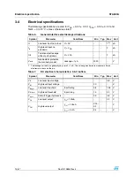

STA309A
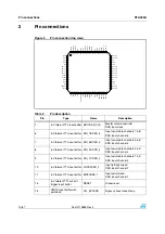
Pin connections
Doc ID 13855 Rev 4
11/67
17
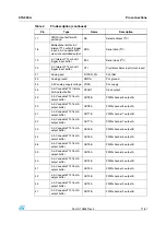
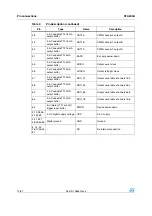
CMOS input buffer with
pull-down
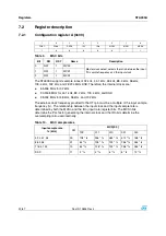
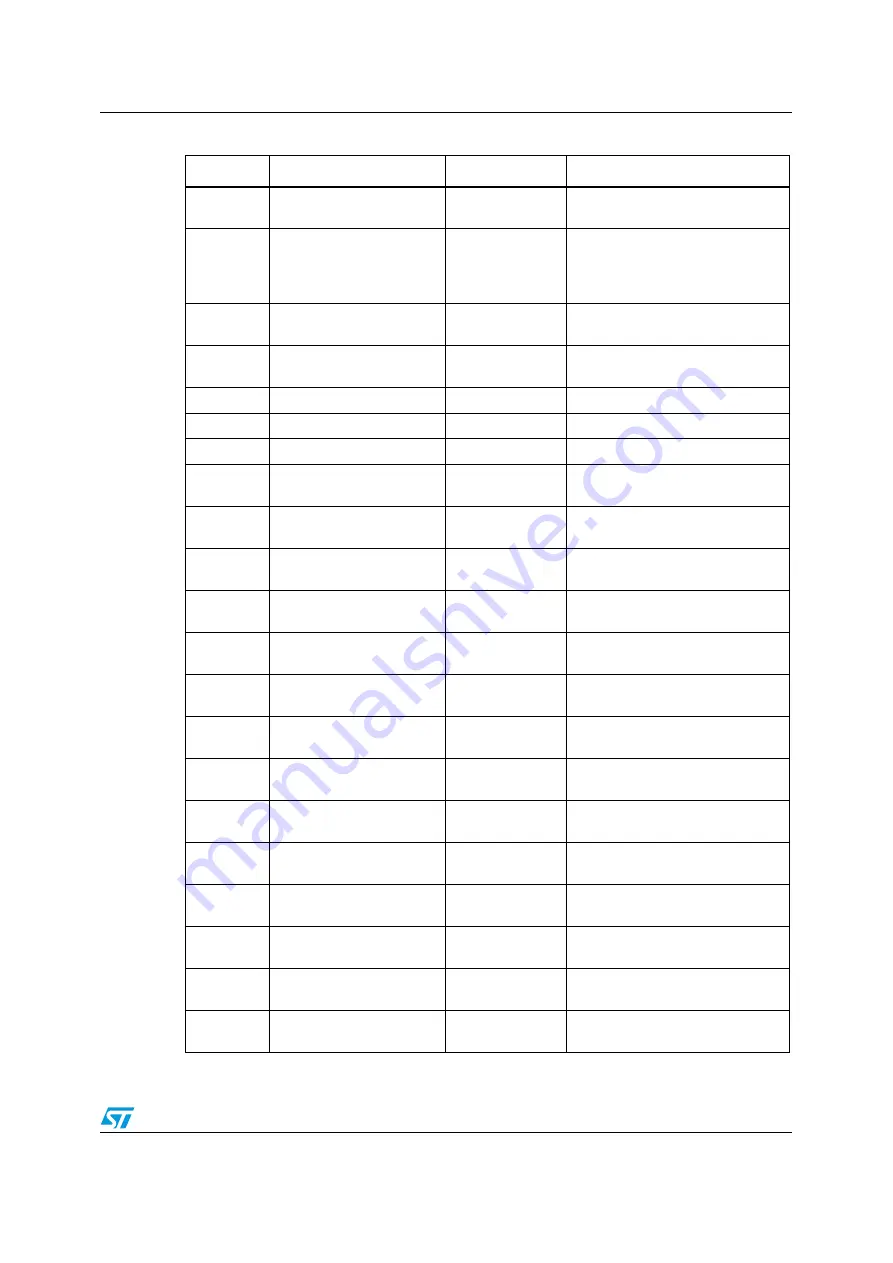
SA
Select address (I
2
C)
18
Bidirectional buffer: 5-V
tolerant TTL schmitt trigger
input; 3.3-V capable 2mA
slew-rate controlled output.
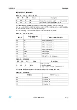
SDA
Serial data (I
2
C)
19
5-V tolerant TTL schmitt
trigger input buffer
SCL
Serial clock (I
2
C)
20
5-V tolerant TTL schmitt
trigger input buffer
XTI
Crystal oscillator input (clock input)
21
Analog pad
FILTER_PLL
PLL filter
23
Analog ground
GNDA
PLL ground
24
3.3V analog supply voltage
VDDA
PLL supply
25
3.3-V capable TTL tristate
4mA output buffer
CKOUT
Clock output
29
3.3-V capable TTL 16mA
output buffer
OUT8B
PWM channel 8 output B
30
3.3-V capable TTL 16mA
output buffer
OUT8A
PWM channel 8 output A
31
3.3-V capable TTL 16mA
output buffer
OUT7B
PWM channel 7 output B
32
3.3-V capable TTL 16mA
output buffer
OUT7A
PWM channel 7 output A
33
3.3-V capable TTL 16mA
output buffer
OUT6B
PWM channel 6 output B
34
3.3-V capable TTL 16mA
output buffer
OUT6A
PWM channel 6 output A
38
3.3-V capable TTL 16mA
output buffer
OUT5B
PWM channel 5 output B
39
3.3-V capable TTL 16mA
output buffer
OUT5A
PWM channel 5 output A
40
3.3-V capable TTL 16mA
output buffer
OUT4B
PWM channel 4 output B
41
3.3-V capable TTL 16mA
output buffer
OUT4A
PWM channel 4 output A
42
3.3-V capable TTL 16mA
output buffer
OUT3B
PWM channel 3 output B
43
3.3-V capable TTL 16mA
output buffer
OUT3A
PWM channel 3 output A
47
3.3-V capable TTL 16mA
output buffer
OUT2B
PWM channel 2 output B
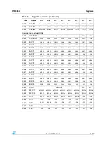
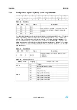
Table 2.
Pin description (continued)
Pin
Type
Name
Description


