7.1.2
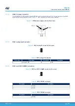
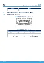
CN4 external I
2
C connector
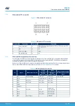
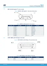
Figure 11.
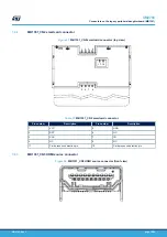
CN4 external I
2
C connector
1
7
2
8
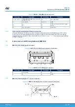
Table 22.
CN4 external I
2
C connector
Pin number
Description
Pin number
Description
1
I2C1_SDA (PB7)
5
PWR (Defined by daughterboard on CN3, or VDD when short CN3
pin17 and pin18)
2
NC
6
NC
3
I2C1_SCL (PB6)
7
GND
4
EX_RESET(PC0)
8
NC
7.1.3
CN2 and CN3 daughterboard connectors
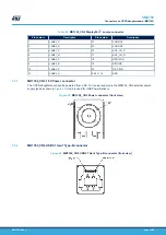
The two CN2 and CN3 18-pin male headers are designed to connect with the legacy peripheral daughterboard
or the UCPD daughterboard to the STM32 G0 Evaluation mother board (MB1581). All GPIOs are available on
CN2/CN3 connectors, and on CN9/C10 extension connectors.
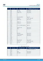
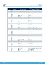
Each pin on CN2 and CN3 can be used by a daughterboard after disconnecting it from the corresponding function
block on the STM32G0C1E-EV Evaluation board. Refer to
for details.
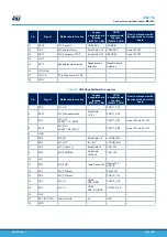
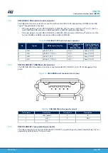
Table 23.
CN2 daughterboard connector
Pin
Signal
Mother board function
Legacy
daughterboard
function
(MB1351_CN5)
UCPD
daughterboard
function
(MB1352_CN9)
How to disconnect with
function block on mother
board
1
PA1
MC_BusVoltage
LDR_OUT
DCDC_EN
Keep JP6 OFF
2
PA15
-
SmartCard RST
USB3_DET
-
3
PB6
I2C1_SCL
I2C1_SCL
I2C1_SCL
-
4
PB7
I2C1_SDA
I2C1_SDA
I2C1_SDA
-
5
GND
-
-
-
-
6
RESET#
-
-
-
-
7
PC6
MC_ENA
IR_IN
Display port
HPD_SOURCE
-
8
PB13
-
I2C2_SCL
DISCHARGE 1
-
9
PB14
-
I2C2_SDA
DISCHARGE 2
-
10
PB1
MC_PFCpwm
-
VSENSE 1
-
UM2783
Connectors on mother board (MB1581)
UM2783
-
Rev 1
page 28/59

