Full wave rectifier
UM1955
10/28
DocID028405 Rev 1
4
Full wave rectifier
The full wave rectifier configuration allows rectification of an input signal. This means that by
defining a reference voltage with a potentiometer, all signals below it will become positive.
When the voltage goes above the reference, the output voltage will not change.
4.1 Schematic
diagram
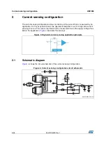
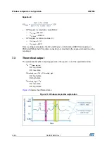
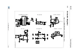
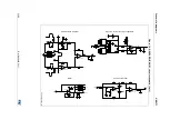
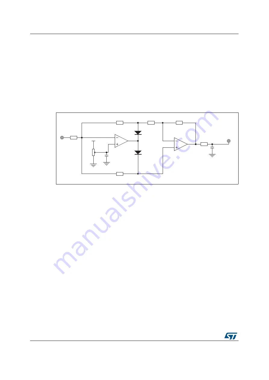
Figure 5
shows the circuit schematic of the full wave rectifier configuration.
Figure 5. Full wave rectifier configuration circuit schematic
4.2
How to set up the board
The input signal must be connected to the Rect_in pin within the rectifier expansion board
section. Similarly, the output signal is available on the Rect_out pin. The output voltage of
the rectifier structure is not intended to be connected to any microcontroller input on the
board since this configuration is most often connected to another analog block.
4.3 Theoretical
output
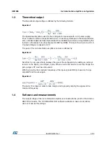
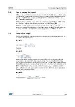
Thus, we have two formulas to define this configuration:
If V
in
< V
ref
: V
out
= 2V
ref
- V
in
If V
in
≥
V
ref
: V
out
= V
in
The V
ref
voltage can be tuned using the P1 potentiometer.
4.4 Measurement
example
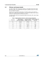
Input voltage = -1 V
V
ref
= 0.5 V
Thus, V
out
= 2 V
$
.
'
N
3
9&&
*1'
*1'
*1'
$
.
'
769,37%
769,37&
N
5
N
5
N
5
N
5
N
5
N
5
S)
&
)
&
5HFWBRXW
5HFWBLQ
*63*',


