


2
Schematic diagrams
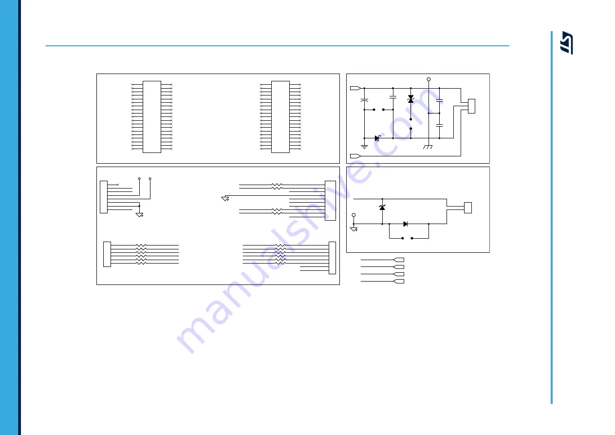
Figure 5.
X-NUCLEO-OUT08A1 circuit schematic (1 of 2)
J1
5
27
16
IN1
36
1
2
DIAG
R121 100 (N.M.)
1
1
R125 100 (N.M.)
16
Arduino Connectors
OUT_FB
PA9
2
17
OUT1
Nch-DRV
11
6
R101 100
6
J3
4
Nch-DRV
20
3
12
8
38
2
2
14
31
19
10
9
CN5
SSQ-110-04-F-S
Alternate Nucleo Supply
7V - 12 V
+
3
DIAG
1
23
3
18
5
22
8
5
1
35
17
Not Assembly
OUT_FB
7
3
PB5
PC7
21
31
ALTERNATE USE
R124 100 (N.M.)
13
9
2
PB0
PC0
PA5
24
2
34
R104 100
Nch-DRV
4
13
6
CN9
SSQ-108-04-F-S
3V3
J2
R133 100 (N.M.)
Nch-DRV
7
R111 100 (N.M.)
Analog supply
8V - 60 V
OUT_FB
33
VIN
R103 100
C3
2.2uF
PA1
PB4
PA3
8
ALTERNATE USE
4
5
OUT_FB
R102 100
21
TP9
5001
24
4
OUT_FB
26
DIAG
R112 100 (N.M.)
20
R123 100 (N.M.)
IN1
OUT_FB
DIAG
2
7
5
default open
VIN
EARTH
D2 BAT48 (N.M.)
IN1
25
ALTERNATE USE
ALTERNATE USE
DEFAULT
ALTERNATE USE
ALTERNATE USE
ALTERNATE USE
ALTERNATE USE
ALTERNATE USE
3
Nch-DRV
4
2
19
35
IN1
10
30
38
C8
47uF (N.M.)
DIAG
26
28
4
10
5V
6
CN7
SSQ-119-04-L-D (N.M.)
2
8
22
DEFAULT
DEFAULT
ALTERNATE USE
36
1
32
7
12
DIAG
TP8
5001
IN1
ALTERNATE USE
Nch-DRV
3v3
30
7
CN6
SSQ-108-04-F-S
18
32
C1
4700pF
3
6
1
STPS1H100A
37
3
15
9
VCC
GND
U2
SM15T39CA
2
1
OUT1
6
PA7
PC1
15
ALTERNATE USE
29
5v0
AVDD
IOREF
R122 100 (N.M.)
33
Morpho Connectors
(N.M.)
R131 100 (N.M.)
IN1
default closed
default open
5
CN2
Con2
14
25
R130 100 (N.M.)
28
C2
4700pF
34
R132 100 (N.M.)
37
CN1
Con3
PB8
PA10
PA4
PA2
PB9
PA0
PB10
CN8
SSQ-106-04-F-S
29
8
PA8
PA6
PB6
(7V-12V NUCLEO supply voltage)
R134 100 (N.M.)
VCC
11
27
23
1
1
U3
ESDA15P60-1U1M (N.M.)
CN10
SSQ-119-04-L-D (N.M.)
NRST
D1
PB3
DEFAULT
UM2715
-
Rev 1
page 7/15
UM2715
Schematic diagrams


