background image


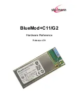
C11/G2 

Hardware Reference 

Release r09 


Summary of Contents for BlueMod+C11/G2 Series

Page 1: ...BlueMod C11 G2 Hardware Reference Release r09...

Page 2: ...es may occur due to individual differences between such devices Product samples were tested in a ref erence environment for compliance with the legal requirements applicable to the reference environme...

Page 3: ...6 Alternate GPIO IO Functions 15 3 6 1 Master Slave SPI Interface 16 3 6 2 Synchronous Serial Interface 16 3 6 3 Multi Channel PWM Controller 17 3 6 4 Analog to Digital Converter 17 3 7 Bluetooth Rad...

Page 4: ...5 7 Wake up Time 30 6 Mechanical Characteristics 31 6 1 Dimensions 31 6 2 Connectors 31 6 3 Recommended Land Pattern 32 6 4 Soldering Temperature Time Profile for lead free re flow soldering 33 6 5 Ho...

Page 5: ...09 www stollmann de Page 5 of 54 7 6 1 NCC Certificate 45 7 6 2 NCC Warning in Chinese 45 7 7 Bluetooth Qualification 46 7 8 RoHS Declaration 47 8 Related Documents 48 9 Packing 49 9 1 Package Label 5...

Page 6: ...C11 G2 can be integrat ed into customer systems It addresses developers of hardware environments for BlueMod C11 G2 For detailed information about software interfaces refer to the software reference m...

Page 7: ...Full Bluetooth data rate up to 2178 kbps asymmetric Support for very low power modes sleep and deep sleep Full 8 to 128 bit encryption High sensitivity design 87 dBm typ Extra ARM7TDMI CPU for embedd...

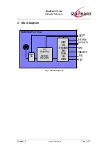
Page 8: ...e Release r09 www stollmann de Page 8 of 54 2 Block Diagram ARM7 CPU AT91SAM7S 256k FLASH 64k SRAM Bluetooth BC04 ROM 3V3 EXT RES RS 232 TTL BlueMod C11 G2 Class1 PA HCI SingleChip 3V3 PA GPIO USB2 0F...

Page 9: ...3 PA Supply for RF Amplifier C 14 GND Reference Supply C 15 GND Reference Supply The pin order is made such that on the customer hardware directly at the pins of each supply pair pins C 13 C14 and pin...

Page 10: ...see sample implementation Stollmann reference design BlueMod Eval C11 G2 Excessive noise or too slow current transient response on the supply rails may have an impact on the RF performance 3 2 Power...

Page 11: ...g EXT RES at 0 3V for 10ms A 74LVC14 Schmitt Trigger gate with a 1kR5 10nF low pass filter at the input is implemented to avoid false reset pulse recognition due to EMC effects If EXT RES is not used...

Page 12: ...hows the deviation in percent of the standard data rates The deviation is caused by the inaccuracy of the crystal oscillator Data Rate bits s Deviation 300 0 5 600 1200 2400 4800 9600 19200 38400 5760...

Page 13: ...uggest the MAX3491E from Maxim Integrated Products due to it sup ports full duplex transmissions UART_RX UART_TX BlueMod C11 G2 ConnectionsinFull DuplexMode D R RO RE DI DE GND A B Z Y VCC GND 2 3 4 5...

Page 14: ...BlueMod C11 G2 Hardware Reference Release r09 www stollmann de Page 14 of 54 CTS Tbd b ytes max Tbd TXD RTS Tbd h t Tbd S RXD Figure 4 UART Timing Diagram...

Page 15: ...p resistor function push pull or open drain Please see specific applica tion software documentation for details After reset all GPIOs have pull ups ac tivated GPIO10 GPIO8 and TXD have 50kR to 300kR p...

Page 16: ...l Interface The Synchronous Serial Interface is capable of handling the protocols I2S Short Frame Sync Long Frame Sync and other Telecom protocols Receiver and trans mitter do act independently Due to...

Page 17: ...IO5 PWM0 PWM Waveform Out CH0 OUT C5 CTS PWM1 PWM Waveform Out CH1 OUT A5 GPIO1 PWM1 PWM Waveform Out CH1 OUT C2 GPIO15 PWM1 PWM Waveform Out CH1 OUT C4 RTS PWM2 PWM Waveform Out CH2 OUT A4 GPIO0 PWM2...

Page 18: ...3 The BlueMod C11 G2 AP variant presents a 50 impedance antenna interface on pin A 27 with adjacent GND pins A 26 and A 28 In this case Pin A 26 and A28 shall be connected directly to the reference GN...

Page 19: ...G2 Hardware Reference Release r09 www stollmann de Page 19 of 54 4 Pin Description The BlueMod C11 G2 module is soldered on customers PCB via stamp pins locat ed on the module PCB edges 4 1 Pin Number...

Page 20: ...O Debug Uart Input A16 GPIO16 I O PU General Purpose IO A17 reserved do not connect A26 ANT_GND Antenna ground connect directly to plane A27 ANT 50 Ohm Rx Tx connection to antenna A28 ANT_GND Antenna...

Page 21: ...TE mode output in DCE mode C3 GPIO13 RTC IN I PU L DTR in DCE mode DSR in DTE mode C4 RTS I PU L Request to send C5 CTS O L Clear to send C6 RXD O Receive Data C7 TXD I Transmit Data C8 GPIO6 RI I O P...

Page 22: ...Exposure to absolute maximum rated con ditions for extended periods may affect device reliability Item Symbol Absolute Maximum Ratings Unit Supply voltage Vcc 3 7V with respect to GND to 0 4V with res...

Page 23: ...7 2400 2483 5 MHz Load impedance Pin A 27 or UMP connector Measured with network ana lyzer in the frequency range at antenna pin 50 Output return loss Pin A 27 or UMP connector Receive Mode to 50 load...

Page 24: ...3 3 USB Pins Vcc 3 3V Tamb 40 C to 85 C Symbol Item Condition Limit Unit Min Max VIL Low Level Input Voltage 0 8 V VIH High Level Input Voltage 2 0 V VDI Diff Input Sensitivity 0 2 V VCM Common Mode...

Page 25: ...ooth RF is activated every 1 25 seconds paging requests from other Blue tooth devices will be recognized after that intervals and accepted if allowed Addi tionally rising control line DTR will activat...

Page 26: ...l DTR ON 8 5 145 mA Idle Page Scan PWD 0 BPSM 2 Signal DTR ON 7 5 65 mA Idle Inquiry Scan PWD 0 BPSM 1 Signal DTR ON 8 0 145 mA Bluetooth connected no data traffic max TX PWR Slave CBT Normal Connecti...

Page 27: ...R with DH5 20 0 0 20 dBm Maximum received signal at 0 1 BER with EDR2 PI 4 DQPSK 20 0 12 0 20 dBm Maximum received signal at 0 1 BER with EDR3 8DPSK 20 0 18 0 20 dBm C I co channel a 9 2 11 11 dB Adja...

Page 28: ...uencies 0 5 dB RF transmit power at antenna Class 1 device EDR2 PI 4 DQPSK b PPK BT Specification 2 402 DPSK 1 9 dBm 2 441 DPSK 1 1 2 480 DPSK 0 5 RF transmit power at antenna Class 1 device EDR3 8DPS...

Page 29: ...BlueMod C11 G2 Hardware Reference Release r09 www stollmann de Page 29 of 54 5 5 1 Antenna Gain and Radiation Pattern Peak Antenna Gain is appr 2dBi...

Page 30: ...nds by parameter change 5 7 Wake up Time The time until the BlueMod C11 G2 is able to process commands coming from a sleep state deep sleep state DTR CTS RX ser i al com m and ___________________ 180...

Page 31: ...n de Page 31 of 54 6 Mechanical Characteristics 6 1 Dimensions 20 0 0 1 0 1 20 4 0 0 0 2 0 15 0 1 0 1 47 5 0 1 0 1 0 15 0 1 0 1 0 1 3 35 0 25 0 25 6 2 Connectors Except for the stamp pins A 1 17 26 28...

Page 32: ...od C11 G2 Hardware Reference Release r09 www stollmann de Page 32 of 54 6 3 Recommended Land Pattern Land pattern recommended for manual soldering Alternative land pattern recommended for reflow solde...

Page 33: ...ow profile recommendation for his product For lead free solder Soldering Temperature Time Profile for reflow soldering Preheat Main Heat Peak tsmax tLmax tpmax Temperature Time Temperature Time Temper...

Page 34: ...idelines The individual case must be checked to decide whether a specific housing is suita ble for the use of the internal antenna A plastic housing must at least fulfill the fol lowing requirements 1...

Page 35: ...sing an external Antenna the antenna is fixed and cannot be removed or replaced by the end user The performance of the internal antenna respectively the external antenna has in any case to be checked...

Page 36: ...target PCB is in the upper right corner This position is optimal concerning antenna interference radiation pat tern and PCB space that has to be keep free for the restricted area recomendable placemen...

Page 37: ...EN 62479 2010 the BlueMod C11 G2 is not intended to be used in close proximity to the human body Please refer to above mentioned regulation for more specific information In respect to the safety regul...

Page 38: ...BlueMod C11 G2 Hardware Reference Release r09 www stollmann de Page 38 of 54 7 Approvals Certifications 7 1 EC Declaration of conformity...

Page 39: ...BlueMod C11 G2 Hardware Reference Release r09 www stollmann de Page 39 of 54 7 2 FCC Grant...

Page 40: ...BlueMod C11 G2 Hardware Reference Release r09 www stollmann de Page 40 of 54 7 3 IC Grant...

Page 41: ...ential installa tion This equipment generates uses and can radiate radio frequency energy and if not installed and used in accordance with the instructions may cause harmful inter ference to radio com...

Page 42: ...oduct integrating the BlueMod C11 G2 must be labeled with at least the following information This device contains transmitter with FCCID RFR C11G2 IC ID 4957A C11G2 Since the BlueMod C11 G2 is a modul...

Page 43: ...BlueMod C11 G2 Hardware Reference Release r09 www stollmann de Page 43 of 54 7 5 Japanese Certification...

Page 44: ...BlueMod C11 G2 Hardware Reference Release r09 www stollmann de Page 44 of 54...

Page 45: ...BlueMod C11 G2 Hardware Reference Release r09 www stollmann de Page 45 of 54 7 6 Taiwanese NCC Certification 1 2 CCAI14LP1850T1 7 6 1 NCC Certificate 7 6 2 NCC Warning in Chinese...

Page 46: ...ID is 7926 For further information about marking requirements of your product attention should be paid the Bluetooth Brand Usage Guide at https www bluetooth org en us bluetooth brand bluetooth brand...

Page 47: ...BlueMod C11 G2 Hardware Reference Release r09 www stollmann de Page 47 of 54 7 8 RoHS Declaration...

Page 48: ...Related Documents ATMEL data sheet AT91SAM7Sxxx Rev F CSR product data book BlueCoreTM 4 ROM BC41B143A April 2006 Radiall UMP MMP Introduction Radiall data sheet UMP R107 103 020Stollmann BlueRS SPP...

Page 49: ...BlueMod C11 G2 Hardware Reference Release r09 www stollmann de Page 49 of 54 9 Packing The BlueMod C11 G2 modules are packed using carrier tape...

Page 50: ...c ddddd dd wwyy q BNDLxxxxxxxxxxxx FCCID RFR C11G2 IC 4957A C11G2 T D11 0008202 R202WW11132841 CCAI14LP1850T1 Note FCC IC MIC and NCC ID s do apply for AI variants only Field Description name Name of...

Page 51: ...lueMod C11 G2 AI SPP Internal 52672 50 BlueMod C11 G2 AP SPP 1 External 52742 50 BlueMod C11 G2 AI BCN Internal 53163 50 SPP Evaluation Kit BlueEva C11 G2 SPP Internal 52743 1 Other variants on reques...

Page 52: ...e Info 20cm instead of 2 5cm FCC PCC1 15 04 2009 AA 5 5 Receiver Sensitivity min Value 6 4 Soldering Temperature Time Profile for lead free re flow soldering in accordance with IPC 20 04 2009 JW corre...

Page 53: ...d re test requirements for the End Product Restricted FCC IC compliance to AI variants in note 1 2 Applications Removed variant BlueMux 3 4 1 Baudrate added 10 Ordering Information MOQs and variant Bl...

Page 54: ...ference Release r09 www stollmann de Page 54 of 54 Stollmann Entwicklungs und Vertriebs GmbH Mendelssohnstra e 15 D 22761 Hamburg Germany Phone 49 0 40 890 88 0 Fax 49 0 40 890 88 444 E mail info stol...

Reviews: