S/AI
Hardware Reference
Page 19 of 52
3.9 Slow Clock Interface
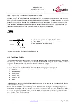
Even though an external slow clock is not required for BLE operation, consumption of power during
power-down modes can be reduced by feeding the module with an optional 32,768 kHz slow clock
at pin XL-IN/SLCK, or connecting an XTAL (32,768kHz) and two capacitors C1, C2 at pins XL-IN
and XL-OUT.
3.9.1 SLCK Specification (External Supplied Signal)
•
32,768 kHz +/-250ppm; duty cycle 30...70%.
•
Signal may be a sine wave, a clipped sine wave, a square wave or a rail-to-rail digital
signal. The amplitude must be at least 200mV
pp
. DC offset is not an issue as long as the
input voltage is between VSS and VDD at all times.
•
connect signal SLCK to XL-IN/SLCK (A6) and leave XL-OUT (A5) open
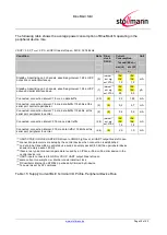
3.9.2 32,768 kHz Crystal Oscillator Specification (32k XOSC)
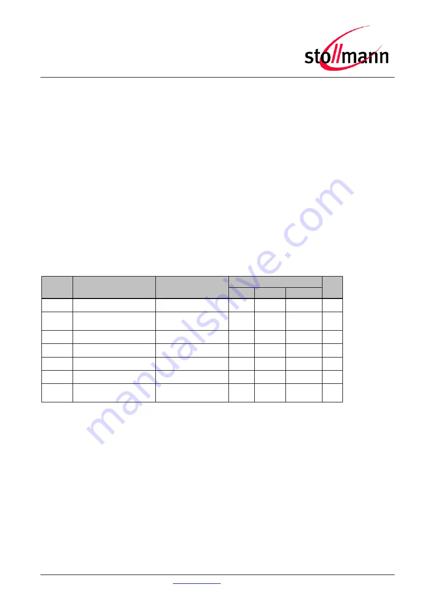
Symbol Item
Condition
Limit
Unit
Min
Typ
Max
f
NOM
Crystal Frequency
T
amb
= 25°C
32,768
kHz
f
TOL
Frequency Tolerance for
BLE applications
including temperature
and aging
(1)
+/-250
ppm
C
L
Load Capacitance
9
12,5
pF
C0
Shunt Capacitance
2
pF
R
S
Equivalent Series Resistor
50
80
k
Ω
P
D
Drive Level
1
µW
C
pin
Input Cap. on XL-IN and
XL-OUT
4
pF
(1)
adjust crystal frequency by choosing correct value for C1, C2 (value depends on C
L
of crystal
and layout)
Table 4: 32,768kHz Crystal Oscillator
The module’s firmware will detect the presence of a slow clock during the boot process and switch
behavior appropriately.


