S/AI
Page 21 of 52
3.11 Operating in a Power-Switched Environment
A potential "back feeding" problem may arise, if the module is operated in an environment where
its power supply (VSUP) is switched off by the application. This might be done to save some power
in times Bluetooth is not needed.
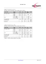
As stated in Table 7, the voltage on any I/O pin must not exceed VSUP by more than 0,3V at any
time. Otherwise some current I
INJ
flows through the internal protection diodes. This may damage
the module (please refer to chapter 5.1 for limits).
There is no problem if the application circuit design and programming can assure that all signals
directed towards S are set to low (U < 0,3V) before and while VSUP is turned off. If this
is not guaranteed, at least a series resistor (about 1k) must be inserted into each signal path. This
does protect the module but obviously cannot prevent from an unwanted, additional current flow in
case of such signal being at high-level. It may be necessary to use driver chips in such appli-
cations, that gate off these signals while VSUP is not present.
3.12 Serial Wire Interface
The Serial Wire interface (SWDIO, SWCLK) is normally not used in a customer’s product. It is
reserved for debugging purposes.
Leave SWDIO, SWCLK unconnected. Only if you intend to use them for debugging purposes,
make them available. Please be aware of the nRF51822 pin sharing SWDIO/nRESET (refer to [1]).
On the S module, pin EXT-RES# is decoupled from SWDIO by a 150
Ω resistor; SWDIO
is connected directly to pin SWDIO/nRESET of the nRF51822 chip. Nevertheless, avoid
driving
EXT-RES# to any logic level while in debug mode, since EXT-RES# will also be driven by the
S or the debugger, when SDIO is driven by either of these.
During any debugging session the external pushbutton reset functionality is not available. Please
use the correct reset options of your serial wire debugger. Alternatively, power-off the system,
remove the debugger and power-up again (refer to [1], Chapter 10 Debugger Interface (DIF)).


