background image


SR/AI 

SR/AP 

Hardware Reference 

Release r09 

www.stollmann.de


Page 3 of 76 


Table of contents 

1


Introduction .............................................................................................................................. 8


1.1


Feature Summary ............................................................................................................. 8


1.2


Applications ...................................................................................................................... 9


1.2.1


General Cable Replacement ...................................................................................... 9


1.2.2


Industry ...................................................................................................................... 9


1.2.3


Automotive ................................................................................................................. 9


1.2.4


Healthcare and Medical ............................................................................................. 9


1.2.5


Sports and Fitness ................................................................................................... 10


1.2.6


Entertainment .......................................................................................................... 10


2


Block Diagram ....................................................................................................................... 11


3


Application Interface .............................................................................................................. 12


3.1


Power Supply ................................................................................................................. 12


3.2


Power-up / -down Slew-Rate .......................................................................................... 12


3.3


Reset .............................................................................................................................. 12


3.4


Supply Voltage Monitor ................................................................................................... 14


3.5


Serial Interface................................................................................................................ 15


3.5.1


3-Wire Serial Interface ............................................................................................. 16


3.5.2


Baud Rate Deviation ................................................................................................ 18


3.6


GPIO Interface ................................................................................................................ 20


3.7


I

2

C Interface .................................................................................................................... 20


3.8


NFC Support ................................................................................................................... 20


3.9


SPI Serial Peripheral Interface ........................................................................................ 21


3.10


Bluetooth Radio Interface ............................................................................................... 22


3.11


WLAN Coexistence Interface .......................................................................................... 22


3.12


Slow Clock Interface ....................................................................................................... 23


3.13


Test Mode Enable ........................................................................................................... 23


3.14


Pin Strapped System Memory Boot Mode Invocation ..................................................... 23


3.15


Operating in a Power-Switched Environment .................................................................. 24


3.16


Serial Wire DEBUG Interface .......................................................................................... 24


3.17


TRACE Interface ............................................................................................................. 24


4


Module Pins ........................................................................................................................... 25


Summary of Contents for BlueMod+SR/AI

Page 1: ...BlueMod SR AI BlueMod SR AP Hardware Reference Release r09 ...

Page 2: ... to individual differences between such devices Device samples were tested in a reference environment for compliance with the legal requirements applicable to the reference environment No representation is made regarding the compliance with legal regulatory or other requirements in other environments No representation can be made and no warranty can be assumed regarding the suitability of the devi...

Page 3: ...upply 12 3 2 Power up down Slew Rate 12 3 3 Reset 12 3 4 Supply Voltage Monitor 14 3 5 Serial Interface 15 3 5 1 3 Wire Serial Interface 16 3 5 2 Baud Rate Deviation 18 3 6 GPIO Interface 20 3 7 I2 C Interface 20 3 8 NFC Support 20 3 9 SPI Serial Peripheral Interface 21 3 10 Bluetooth Radio Interface 22 3 11 WLAN Coexistence Interface 22 3 12 Slow Clock Interface 23 3 13 Test Mode Enable 23 3 14 P...

Page 4: ...uding EXT RES 30 5 6 Power Consumption and Power Down Modes 33 5 6 1 Classic Bluetooth 33 5 6 2 LE Configurations 34 5 6 2 1 LE Operating in Peripheral Device Role 34 5 6 2 2 LE Operating in Central Device Role 35 5 7 RF Performance 37 5 7 1 GFSK PI 4 DQPSK 8DPSK Receiver 37 5 7 2 GFSK PI 4 DQPSK 8DPSK Transmitter 40 5 7 3 BLE Receiver 43 5 7 4 BLE Transmitter 44 5 7 5 Antenna Gain and Radiation P...

Page 5: ... Requirements for the End Product 59 8 3 IC Compliance 59 8 3 1 IC Grant 60 8 3 2 IC Statement 61 8 3 3 IC Caution 61 8 3 4 IC RF exposure Statement 61 8 3 5 IC Labeling Requirements for the End Product 62 8 3 6 IC Label Information BlueMod SR 62 8 4 KCC Certification Grant 63 8 5 MIC Certification 64 8 6 Bluetooth Qualification 68 8 7 RoHS Declaration 69 9 Related Documents 69 10 Packing 70 10 1 ...

Page 6: ...stence 22 Figure 11 BlueMod SR Pin Numbering Top View 25 Figure 12 Typical Antenna Radiation Pattern at 2402MHz 46 Figure 13 Typical Antenna Radiation Pattern at 2441MHz 47 Figure 14 Typical Antenna Radiation Pattern at 2480MHz 47 Figure 15 BlueMod SR AI dimensions 49 Figure 16 BlueMod SR AP dimensions 49 Figure 17 BlueMod SR Land Pattern 50 Figure 18 Soldering Temperature Time Profile For Reflow ...

Page 7: ...Supply Current BLE Terminal I O Profile Peripheral Device Role Standby 34 Table 16 Supply Current BLE Terminal I O Profile Peripheral Device Role CI 7 5ms 34 Table 17 Supply Current BLE Terminal I O Profile Peripheral Device Role CI 37 5ms 34 Table 18 Supply Current BLE Terminal I O Profile Central Device Role Standby 35 Table 19 Supply Current BLE Terminal I O Profile Central Device Role CI 7 5ms...

Page 8: ...e Fully qualified Bluetooth V4 0 Dual Mode BR EDR LE CE certified FCC IC and KCC certified CSR8811 BlueCore08 and Application Processor inside Complete Co location and Co existence with 802 11 AFH Unity 3e Fast Connection Setup RF output power up to 7dBm with power control Supply Voltage range 2 5V to 3 6V typical 3 3V Internal crystal oscillator 26 MHz and 14 7456 MHz LGA Surface mount type BlueM...

Page 9: ...cure 1 2 2 Industry Typical Bluetooth application include scanner printer as well as automation controls In the automation application area Bluetooth is mainly used for transport of I O signals Bluetooth low energy can be used to monitor and control motors actuators values and entire processes 1 2 3 Automotive Modules are mainly used in aftermarket application like personal navigation devices head...

Page 10: ...itors body temperature thermometers pedometers cadence meters altimeter positioning GPS tracking and watches displaying information from sensors 1 2 6 Entertainment Bluetooth technology is already used in a wide variety of devices in the entertainment sector namely set top boxes gaming consoles Bluetooth low energy is expected to further increase the use of Bluetooth technology in devices like TV ...

Page 11: ...BlueMod SR BP Filter RESET I2C UART GPIO SPI WLAN COEX 1 2 7 3 4 GND 3 3V 26MHz 14 7456MHz opt 32kHz 9 EEPROM DEBUG onboard antenna EXT ANT 1 2 1 BlueMod SR AI only 2 BlueMod SR AP only TRACE Figure 1 BlueMod SR Block Diagram Note BlueMod SR AI has an internal ceramic antenna whereas BlueMod SR AP provides for an 50Ω RF interface ...

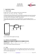
Page 12: ...cannot be placed close to the BlueMod SR it is recommended to place an additional low ESR capacitor with at least 10µF as close as possible to the VSUP pins E 6 F 6 or C 1 BlueMod SR XC6204 3 3 C 1 E 6 F 6 VSUP GND A 7 E 7 F 7 B 5 8 C 5 8 D 8 E 8 F 8 10µ 100n 1n 1µ VOUT VSS VIN CE 5 1 3 2 5VDC Figure 2 BlueMod SR Example Power Supply 3 2 Power up down Slew Rate Parameter Min Max Unit VSUP rise tim...

Page 13: ...t used it may be left open Note EXT RES pin can also be output Use an open drain device or push button to drive it low EXT RES must not be connected to VSUP or driven to logic high level directly Provide for a 1kΩ series resistor when driving EXT RES from a CMOS output BlueMod SR C 1 E 6 F 6 VSUP GND 3V3 EXT RES B 1 Reset Switch is optional Please Note BlueMod SR has an open drain output and appro...

Page 14: ... pull up 2 WLAN DNY Input with weak pull up 2 BT PER Input with weak pull up 2 TESTMODE Input floating BOOT0 Input with pull down resistor 100kΩ 4 SWDIO Input with pull up 1 SWCLK Input with pull down 1 1 pull up pull down RPU RPD is typ 40kΩ 30kΩ to 50kΩ 2 weak pull up pull down See Table 12 DC characteristics digital IO CSR8811 related 3 strong pull up pull down See Table 12 DC characteristics d...

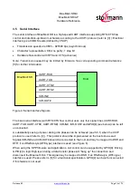
Page 15: ...als The basic serial interface with RTS CTS flow control uses only four signal lines UART RXD UART TXD UART CTS UART RTS IUR IN IUR OUT and GPIO 4 see below can be left unconnected A substantially saving of power during idle phases can be achieved see 5 6 1 when the UICP protocol is used refer to 3 This protocol should be implemented on the host side as well Signals IUR IN and IUR OUT should be co...

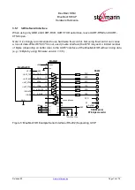
Page 16: ...pending on buffer size to the UART interface of the BlueMod SR without losing data e g 1 kByte by using firmware version 1 310 2 BlueMod SR GND MAX3241 14 3V3 22 23 2 3 7 8 4 6 1 9 TXD RXD RTS CTS IUR OUT IUR IN TXD RXD RTS CTS DTR DSR DCD RI RS232 DSUB9 male DTE style connector 9 4 10 5 11 6 7 8 19 13 18 12 17 16 15 F 4 D 2 D 7 F 3 B 4 D 5 UART_TXD UART_RXD UART_RTS UART_CTS IUR OUT IUR IN SHDN E...

Page 17: ...XD UART_TXD UART_CTS UART_RTS 10µ 100n 1n SN74AVC4T245 User Host System VSUP XC6204 3 3 VOUT VSS VIN CE 1µ 100k 100k VCCB 1B1 1B2 2B1 2B2 2A2 2A1 1A2 1A1 VCCA 1DIR 1OE 2DIR 2OE GPIO Out no pu pd GPIO Out no pu pd TXD RTS RXD CTS 5VDC OE_DRV BT_ENABLE VDD_HOST 1 2 3 6V 3V3_switched Figure 6 BlueMod SR Example Serial Interface Mixed Signal Level ...

Page 18: ...o low transitions The following table shows the BlueMod SR baud rate deviation in percent of the standard baud rates caused by the baud rate generator granularity Add 50ppm for the tolerance of the local oscillator over the full temperature range Data Rate bits s Deviation 9600 0 0 19200 0 0 38400 0 0 57600 0 0 115200 0 0 230400 0 0 460800 0 0 921600 0 0 Table 3 Standard Baud Rates and Deviations ...

Page 19: ...16 𝐷𝐼𝑉 𝑀𝐴𝑁𝑇𝐼𝑆𝑆𝐴 If FRACTION 15 MANTISSA MANTISSA 1 FRACTION 0 𝐵𝑅 𝐻𝑧 14 745 600 16 𝑀𝐴𝑁𝑇𝐼𝑆𝑆𝐴 𝐹𝑅𝐴𝐶𝑇𝐼𝑂𝑁 16 𝐷𝑒𝑣𝑖𝑎𝑡𝑖𝑜𝑛 100 𝑚𝑎𝑡ℎ 𝑎𝑏𝑠 𝐶𝐵𝑅 𝐵𝑅 𝐶𝐵𝑅 Explanation of used functions and expressions 1 math floor x returns the largest integer less than or equal to x 2 math round x returns a number of x rounded to the nearest integer 3 math abs x returns the absolute value of x 4 DIV floating variable 5 CBR targete...

Page 20: ...orm an I2 C interface It is required to connect 4k7 pull up resistors on I2C SCL and I2C SDA when this interface is used I2C SCL I2C SDA GPIO 0 I2C SCL GPIO 1 I2C SDA BlueMod SR VSUP Rpu 4k7 3 3V B 2 D 3 C 1 E 6 F 6 3 3V Rpu 4k7 3 3V NXP NT3H1101 Figure 7 BlueMod SR I2 C Interface 3 8 NFC Support2 From SPP firmware version V1 500 on and higher the NFC TAG NXP NT3H1101 will be supported by using th...

Page 21: ...tage and temperature range of the BlueMod SR 3 9 SPI Serial Peripheral Interface3 The serial peripheral interface SPI allows half full duplex synchronous serial communication with external devices The interface can be configured as the master and in this case it provides the communication clock SCK to the external slave device The interface is also capable of operating in multi master configuratio...

Page 22: ...ovides a 50 RF interface It is highly recommended that you follow the design rule given in the Stollmann Application Note on Antenna design 4 3 11 WLAN Coexistence Interface4 For implementing WLAN Coexistence with CSR s Wi Fi solution the Unity 3e scheme could be implemented on request Usage of signal BT_PER is not necessary at the moment BlueMod SR WiFi Device BT ACT BT STAT WLAN DNY BT PER Figur...

Page 23: ... reserved Leave pin TESTMODE open 3 14 Pin Strapped System Memory Boot Mode Invocation Asserting BOOT0 high will invoke the system memory bootloader at start up This is required for firmware update Thus access to this signal and a means to drive it at high level should be foreseen by the customer s hardware While not in use this signal can be left open or driven to logic low level To connect to th...

Page 24: ...es protect the module but obviously cannot prevent from an unwanted additional current flow in case of such signal being at high level It may be necessary to use driver chips in such appli cations that gate off these signals while VSUP is not present 3 16 Serial Wire DEBUG Interface The Serial Wire interface SWDIO SWCLK is normally not used in a customer s product It is reserved for debugging purp...

Page 25: ... r09 www stollmann de Page 25 of 76 4 Module Pins 4 1 Pin Numbering F1 E1 D1 C1 B1 A1 A2 A3 A4 A5 A6 A7 A8 F2 E2 D2 C2 B2 F3 E3 D3 C3 B3 F4 E4 D4 C4 B4 F5 E5 D5 C5 B5 F6 E6 D6 C6 B6 F7 E7 D7 C7 B7 F8 E8 D8 C8 B8 Figure 11 BlueMod SR Pin Numbering Top View ...

Page 26: ... O 5 GPIO 3 I2C SDA D 1 GPIO 2 I O 5 GPIO 3 SPI MOSI E 4 GPIO 3 I O 5 GPIO 3 D 4 GPIO 4 I O 5 GPIO 3 F 2 GPIO 5 I O 5 GPIO 3 SPI MISO C 4 GPIO 6 O PP TRACE UART TXD C 3 GPIO 7 I O 5 GPIO 3 E 2 GPIO 8 I O 5 GPIO 3 SPI SCK A 3 BT ACT O WLAN coexistence A 1 BT STAT O WLAN coexistence A 4 WLAN DNY I PD WLAN coexistence A 2 BT PER O WLAN coexistence F 1 TESTMODE I PU L Testmodi E 1 BOOT0 I PD 1 System ...

Page 27: ...ol refer to 3 D 5 IUR IN IUR IN I PD L UICP Control refer to 3 D 3 GPIO 0 I2C_SCL O OD NFC TAG NXP NT3H1101 I2 C SCL 6 and RSSI output and generic I2C function B 2 GPIO 1 I2C_SDA I O NFC TAG NXP NT3H1101 I2 C SDA 6 and RSSI output and generic I2C function D 1 GPIO 2 IOC I O User IO E 4 GPIO 3 IOB I O User IO D 4 GPIO 4 HANGUP I PD optional refer to 5 F 2 GPIO 5 IOD I O User IO C 4 GPIO 6 reserved ...

Page 28: ...st gives some hints how to handle unused signals EXT RES If no external Reset is needed Leave open BOOT0 leave open SLCK If no external slow clock is provided Leave open or tie to GND UART RTS UART CTS If neither flow control nor UICP is used Leave open IUR OUT IUR IN If UICP is not used leave open BT ACT BT STAT If there is no WLAN device on the same PCB Leave open BT PER WLAN DNY TESTMODE Leave ...

Page 29: ...ded periods may affect device reliability Item Symbol Absolute Maximum Ratings Unit Supply voltage VSUP 0 3 to 3 6 V Voltage on any pin VPin 0 3 to VSUP 0 4 V Table 6 Absolute Maximum Ratings 5 2 Electrical Requirements VSUP 3 3V Tamb 25 C if nothing else stated Item Condition Limit Unit Min Typ Max Frequency Range 2400 2483 5 MHz Load impedance Measured with network analyzer in the frequency rang...

Page 30: ...M32 MCU and CSR8811 do have different electrical I O characteristics All Module I O pins are connected directly to these chips without signal conditioning except for some pull up pull down resistors as indicated Therefore the electrical characteristics are split in different tables STM Related Signals EXT RES additional filter C 100n to GND UART TXD UART RXD UART CTS UART RTS additional pull up re...

Page 31: ...P 3 6V V O H 2 3 V 8 mA RPU weak pull up resistor VIN VSS 30 40 50 kΩ RPD weak pull down resistor VIN VDD 30 40 50 kΩ Ilc I O pad leakage current 3 0 3 A Cl Input Capacitance 5 pF Table 10 DC Characteristics Digital IO STM32 related External Slow Clock SLCK Tamb 25 C Symbol Item Condition Limit Unit Min Typ Max VLSEL Low Level Input Voltage VSUP 2 5 to 3 6V 0 0 0 3 V VLSEH High Level Input Voltage...

Page 32: ...P 0 4 V VOL Low Level Output Voltage IOL 4mA 0 4 V VOH High Level Output Voltage IOH 4mA 0 75xVSUP V Isp u Input current Strong pull up 150 40 10 A Isp d Input current Strong pull down 10 40 150 A Iwp u Input current Weak pull up 5 0 1 0 0 33 A Iwp d Input current Weak pull down 0 33 1 0 5 0 A Ilc I O pad leakage current n a A Cl Input Capacitance 1 0 5 0 pF Table 12 DC Characteristics Digital IO ...

Page 33: ...3V Tamb 25 C Tx Power 7 dBm all GPIO lines left open SLCK 32 768 kHz Condition Note Slow clock SLCK Current Consumption Unit IAvg Standby page scan inquiry scan interval 1 28s internal external 4 2 4 0 mA Standby page scan inquiry scan interval 1 28s UICP active serial Interface down 1 internal external 0 9 0 75 mA Bluetooth connected no data traffic Slave 2 3 14 4 mA Bluetooth connected data traf...

Page 34: ...n 1 internal external 0 4 0 25 0 34 0 2 mA Table 15 Supply Current BLE Terminal I O Profile Peripheral Device Role Standby Condition Note Slow clock SLCK Current Consumption Unit Tx power dBm max 7 min 23 IAvg IAvg Connected connection interval 7 5 ms no data traffic 2 3 6 9 6 8 8 mA Connected connection interval 7 5 ms data traffic 115 kbit s at the serial port central to peripheral 2 6 24 22 mA ...

Page 35: ...average power consumption of BlueMod SR in LE mode operating in the central device role VSUP 3 3V Tamb 25 C all GPIO lines left open SLCK 32 768 kHz Condition Note Slow clock SLCK Current Consumption Unit Tx power dBm max 7 min 23 IAvg IAvg Standby scanning for peripherals 6 50 49 mA Table 18 Supply Current BLE Terminal I O Profile Central Device Role Standby Condition Note Slow clock SLCK Current...

Page 36: ... serial port central to peripheral 2 4 6 16 5 15 mA Table 20 Supply Current BLE Terminal I O Profile Central Device Role CI 37 5ms Notes 2 connection parameters are setup by the central device when connection is established 3 no data to be transmitted central device sends an empty packet 80 bit then peripheral device answers empty packet 80 bit 4 these are a typical connection parameters used by a...

Page 37: ...nnel GFSK 8 11 11 dB Adjacent channel selectivity C I f f0 1MHz GFSK 2 0 0 dB Adjacent channel selectivity C I f f0 1MHz GFSK 1 0 0 dB Adjacent channel selectivity C I f f0 2MHz GFSK 39 30 30 dB Adjacent channel selectivity C I f f0 2MHz GFSK 30 30 20 dB Adjacent channel selectivity C I f f0 3MHz GFSK 45 40 40 dB Adjacent channel selectivity C I f f0 5MHz GFSK 46 40 40 dB Adjacent channel selectiv...

Page 38: ...ed conducted according to BT specification v1 2 2 0 2 0 EDR 2 1 2 1 EDR 3 0 3 0 HS 4 0 Receiver Frequency GHz Limit BT Unit Min Typ Max Spec Sensitivity at 0 1 BER DH1 2 402 84 80 70 dBm 2 441 88 84 2 480 88 84 Sensitivity at 0 1 BER DH5 2 402 84 80 70 dBm 2 441 88 84 2 480 88 84 Sensitivity at 0 1 BER EDR2 PI 4 DQPSK 2 402 88 70 70 dBm 2 441 91 70 2 480 91 70 Sensitivity at 0 1 BER EDR3 8DPSK 2 4...

Page 39: ...80 88 84 Sensitivity at 0 1 BER DH5 2 402 84 80 70 dBm 2 441 88 84 2 480 88 84 Sensitivity at 0 1 BER EDR2 PI 4 DQPSK 2 402 87 70 70 dBm 2 441 90 70 2 480 90 70 Sensitivity at 0 1 BER EDR3 8DPSK 2 402 78 70 70 dBm 2 441 80 70 2 480 80 70 Maximum received signal at 0 1 BER DH1 20 0 20 dBm Maximum received signal at 0 1 BER PI 4 DQPSK 20 0 20 dBm Maximum received signal at 0 1 BER 8DPSK 20 0 20 dBm ...

Page 40: ...device EDR2 π 4 DQPSK b 2 402 GFSK 2 0 TX 4 to 1 dBm 2 402 π 4 DQPSK 0 9 2 441 GFSK 4 7 2 441 π 4 DQPSK 3 7 2 480 GFSK 5 6 2 480 π 4 DQPSK 4 6 RF transmit power 50 Ω load at antenna Class 1 device EDR3 8DPSK b 2 402 GFSK 2 1 TX 4 to 1 dBm 2 402 8DPSK 1 0 2 441 8GFSK 4 8 2 441 8DPSK 3 7 2 480 GFSK 5 6 2 480 8DPSK 4 6 RF power control range 16 30 16 dB RF power range control resolution 2 4 8 2 to 8 ...

Page 41: ... Class 1 device EDR2 π 4 DQPSK b 2 402 GFSK 0 5 TX 4 to 1 dBm 2 402 π 4 DQPSK 1 9 2 441 GFSK 2 5 2 441 π 4 DQPSK 1 2 2 480 GFSK 4 0 2 480 π 4 DQPSK 2 8 RF transmit power 50 Ω load at antenna Class 1 device EDR3 8DPSK b 2 402 GFSK 0 5 TX 4 to 1 dBm 2 402 8DPSK 1 7 2 441 GFSK 2 5 2 441 8DPSK 1 2 2 480 GFSK 4 0 2 480 8DPSK 2 8 20 dB bandwidth for modulated carrier 925 1000 1000 kHz Initial carrier fr...

Page 42: ... dBm 2 402 π 4 DQPSK 0 8 2 441 GFSK 2 8 2 441 π 4 DQPSK 1 7 2 480 GFSK 4 0 2 480 π 4 DQPSK 2 9 RF transmit power 50 Ω load at antenna Class 1 device EDR3 8DPSK b 2 402 GFSK 0 3 TX 4 to 1 dBm 2 402 8DPSK 0 8 2 441 GFSK 2 8 2 441 8DPSK 1 7 2 480 GFSK 4 0 2 480 8DPSK 2 9 20 dB bandwidth for modulated carrier 925 1000 1000 Initial carrier frequency tolerance 75 10 75 75 Carrier frequency drift packet ...

Page 43: ...0 1 MHz 9 15 15 dB F F0 2 MHz 27 17 17 dB F F0 2 MHz 19 15 15 dB F F0 3 MHz 43 27 27 dB F F0 5 MHz 49 27 27 dB F Fimage 24 9 9 dB Maximum level of intermodulation interferers 50 18 50 dBm VSUP 2 5V to 3 6V Tamb 30 C Measured conducted according to BT specification RF PHY TS 4 0 1 Receiver Frequency GHz Min Typ Max BT Spec Unit Sensitivity at 30 8 PER 2 402 87 83 70 dBm 2 440 90 87 2 480 90 87 Repo...

Page 44: ... minimum modulation 185 214 185 kHz f2avg f1avg 0 8 0 83 0 8 Frequency Offset 95 25 95 150 kHz Carrier drift rate 4 20 20 kHz 50µs Carrier drift 5 50 50 kHz VSUP 2 5V to 3 6V Tamb 30 C Measured conducted according to BT specification RF PHY TS 4 0 1 Transmitter Frequency GHz Min Typ Max BT Spec Unit RF transmit Power 2 402 0 5 4 0 10 20 to 10 dBm 2 440 2 5 6 5 10 2 480 3 5 7 5 10 ACP F F0 2MHz 28 ...

Page 45: ...ax BT Spec Unit RF transmit Power 2 402 1 0 4 0 10 20 to 10 dBm 2 440 3 0 6 0 10 2 480 4 0 7 0 10 ACP F F0 2MHz 30 20 30 dBm F F0 3MHz 42 40 30 F F0 3MHz 60 30 30 f1avg maximum modulation 225 267 275 225 f1avg 275 kHz f2max minimum modulation 185 214 185 kHz f2avg f1avg 0 8 0 83 0 8 Frequency Offset 95 25 95 150 kHz Carrier drift rate 5 20 20 kHz 50µs Carrier drift 5 50 50 kHz Table 24 RF Performa...

Page 46: ...rated into an end product while the recommendations depicted in 6 4 Placement Recommendation are maintained the following typical antenna radiation patterns can be expected Radiation Pattern will depend on the end products PCB size masses in the antenna environment housing material and geometrics Figure 12 Typical Antenna Radiation Pattern at 2402MHz Y X Z ...

Page 47: ...od SR AI BlueMod SR AP Hardware Reference Release r09 www stollmann de Page 47 of 76 Figure 13 Typical Antenna Radiation Pattern at 2441MHz Figure 14 Typical Antenna Radiation Pattern at 2480MHz Y X Z Y X Z ...

Page 48: ...BlueMod SR is able to accept link requests or serial data depends on the firmware version In the SPP firmware the module is command ready and Bluetooth links are accepted at least 1 1 s after signal EXT RES is de asserted or VSUPx is in a valid range Note For further information refer to the document BlueMod SR_Startup_Timing 6 ...

Page 49: ...n BlueMod SR 2 5 10 0 0 2 0 0 0 1 0 1 0 1 0 1 0 1 0 1 Verbleibende Stege nach Nutzentrennung remaining break tabs after separation 2 6 Figure 15 BlueMod SR AI dimensions 17 0 0 2 0 0 FCC ID RFRMSR stollmann BlueMod SR 2 5 10 0 0 2 0 0 0 1 0 1 0 1 0 1 0 1 0 1 Verbleibende Stege nach Nutzentrennung remaining break tabs after separation Figure 16 BlueMod SR AP dimensions ...

Page 50: ...e Page 50 of 76 6 2 Recommended Land Pattern F1 E1 D1 C1 B1 A1 A2 A3 A4 A5 A6 A7 A8 F2 E2 D2 C2 B2 F3 E3 D3 C3 B3 F4 E4 D4 C4 B4 F5 E5 D5 C5 B5 F6 E6 D6 C6 B6 F7 E7 D7 C7 B7 F8 E8 D8 C8 B8 1 25 1 25 7x1 5 10 5 5x1 5 7 5 0 9 17 0 10 0 TOP VIEW Figure 17 BlueMod SR Land Pattern ...

Page 51: ...Preheat Main Heat Peak tsmax tLmax tpmax Temperature Time Temperature Time Temperature Time C sec C sec C sec 150 100 217 90 260 10 230 50 Average ramp up rate C sec 3 Average ramp down rate C sec 6 Max Time 25 C to Peak Temperature min 8 Opposite side re flow is prohibited due to module weight Devices will withstand the specified profile and will withstand up to 1 re flows to a maximum temperatur...

Page 52: ...nents on any layer provide solid ground plane s as large as possible around 17 do not place any conductive parts in this area 20 20 40 area Applic PCB Figure 19 BlueMod SR AI Placement Recommendation 6 5 Housing Guidelines The individual case must be checked to decide whether a specific housing is suitable for the use of the internal antenna A plastic housing must at least fulfill the following re...

Page 53: ...ntended to be used in close proximity to the human body Please refer to above mentioned regulation for more specific information In respect to the safety regulation EN60950 1 2006 A11 2009 A1 2010 AC 2011 all conductive parts of the BlueMod SR are to be classified as SELV circuitry OEM s implementing the BlueMod SR in their products should follow the isolation rules given in regulation EN 60950 1 ...

Page 54: ...al slow clock oscillator All other module pins may be left unconnected Host MCU VDD GND 3V3 GPIO o In this example BlueMod SR is connected to an MCU supporting RTS CTS flow control and Hangup Firmware update is supported BOOT0 EXT RES connected The slow clock oscillator 32 768kHz is optional it helps to save power during power down states 1k BlueMod SR AI C 1 E 6 F 6 VSUP GND B 1 EXT RES BOOT0 GPI...

Page 55: ...enna with less than 2dBi gain The actual versions of EU Declaration of Conformity EU DoC can be downloaded from the qualification section on the product page via the following link http www stollmann de en support downloads bluetooth adapter bluemod sr html 8 2 FCC Compliance The BlueMod SR AI has been tested to fulfill the FCC requirements Test reports are available on request Grants of the Full ...

Page 56: ...BlueMod SR AI BlueMod SR AP Hardware Reference Release r09 www stollmann de Page 56 of 76 8 2 1 FCC Grant ...

Page 57: ...BlueMod SR AI BlueMod SR AP Hardware Reference Release r09 www stollmann de Page 57 of 76 ...

Page 58: ... will not occur in a particular installation If this equipment does cause harmful interference to radio or television reception which can be determined by turning the equipment off and on the user is encouraged to try to correct the interference by one or more of the following measures Reorient or relocate the receiving antenna Increase the separation between the equipment and receiver Connect the...

Page 59: ... tested to fulfill the IC requirements Test reports RSS 210 of Industry Canada are available on request Grants of the Full Modular Approval will be shown below For selling products implementing the BlueMod SR AP in Canada you ll have to apply for a Class II Permissive Change from the IC authorities Depending on antenna gain and other factors the IC TCB will issue a reduced test plan for re testing...

Page 60: ...BlueMod SR AI BlueMod SR AP Hardware Reference Release r09 www stollmann de Page 60 of 76 8 3 1 IC Grant ...

Page 61: ...nement principal doivent être enlevés aux frais de leur utilisateur This device complies with Industry Canada license exempt RSS standard s Operation is subject to the following two conditions 1 this device may not cause interference and 2 this device must accept any interference including interference that may cause undesired operation of the device NOTICE This Class B digital apparatus complies ...

Page 62: ...AP must be labeled with at least the following information This device contains transmitter with FCC ID RFRMSR IC ID 4957A MSR 8 3 6 IC Label Information BlueMod SR The BlueMod SR shows no IC ID on the product label because there is no space available IC allows on request to state the IC ID in the product manual This product has been granted to do so Model BlueMod SR The IC ID is 4957A MSR ...

Page 63: ...BlueMod SR AI BlueMod SR AP Hardware Reference Release r09 www stollmann de Page 63 of 76 8 4 KCC Certification Grant ...

Page 64: ...nna configuration requires an administrative Japanese Re certification with reduced costs For using another antenna with variant BlueMod SR AP please contact Stollmann E V GmbH for starting the Japanese administrative process Costs for re measurements and certification should be considered Approved External Antennas List Manufacturer Part Number Gain Connector Approval WIMO 17010 11REV 2 dBi Rever...

Page 65: ...BlueMod SR AI BlueMod SR AP Hardware Reference Release r09 www stollmann de Page 65 of 76 ...

Page 66: ...BlueMod SR AI BlueMod SR AP Hardware Reference Release r09 www stollmann de Page 66 of 76 ...

Page 67: ...BlueMod SR AI BlueMod SR AP Hardware Reference Release r09 www stollmann de Page 67 of 76 ...

Page 68: ...esign ID is 44784 For further information about marking requirements of your product attention should be paid the Bluetooth Brand Usage Guide at https www bluetooth org en us bluetooth brand bluetooth brand According to the Bluetooth SIG rules Bluetooth Declaration Process Document DPD you must complete a Product Listing and Declaration of Compliance DoC referencing the Qualified Design QDID for y...

Page 69: ...n section on product web site via the following link http www stollmann de en support downloads bluetooth adapter bluemod sr html 9 Related Documents 1 CD00171190 pdf Oct 2011 Rev 14 STM32_Reference 2 CD00191185 pdf April 2011 Rev 8 STM32_datasheet 3 Stollmann UICP_UART_Interface_Control_Protocol_r01 pdf 4 Stollmann AppNote_B0601_Antenna_Design_V1_0 pdf 5 Stollmann BlueMod SR AT Command Reference ...

Page 70: ...g von der Rolle pull off direction from reel FCC ID RFRMSR stollmann BlueMod SR FCC ID RFRMSR stollmann BlueMod SR 25 Leertaschen Vorspann pro Verpackungseinheit 25 empty pockets as leader per packing unit 15 Leertaschen Nachspann pro Verpackungseinheit 15 empty pockets as trailer per packing unit FCC ID RFRMSR stollmann BlueMod SR FCC ID RFRMSR stollmann BlueMod SR ...

Page 71: ...09 www stollmann de Page 71 of 76 10 1 Tape The dimensions of the tape are shown in the drawing below values in mm 2 0 0 1 0 1 10 9 0 1 0 1 18 3 0 1 0 1 R 0 5 1 75 0 10 0 10 24 0 0 3 0 3 10x4 0 40 0 0 2 0 2 1 5 0 1 0 0 12 0 11 5 0 1 0 1 0 3 3 0 10 2 Reel tbd ...

Page 72: ...red in Germany XXXXXXXXXXXXXXXX aaaaa aa b c ddddd dd mwwyy q FCC ID RFRMSR IC 4957A MSR MSIP CRM Rfr BlueModSR T D15 0014202 R 202 LSD026 Field Description name Name of product p n Product number firmware Firmware version fw p n Product number of firmware trace Manufacturer M optional Date YearCalendarWeek YYWW quantity Number of contained modules If the label on the package box is different to t...

Page 73: ...units Comments BlueMod SR AI internal 53231 xx 50 BlueMod SR AP external 53252 xx 400 BlueEva SR Internal 53249 xx 1 Evaluation Kits Other variants on request please contact Stollmann sales department 11 2 Standard Packing Unit The standard packing unit is 400 or 1000 pieces on Tape and Reel 11 3 Evaluation Kit The kit BlueEva SR is available to evaluate functionality and start your firmware imple...

Page 74: ...STM32 WAKEUP New chapter 4 3 Handling of Unused Signals Chapter 5 6 Power Consumption and Power Down Modes Tables updated Chapter 5 7 RF Performance RF parameter updated Chapter 5 7 5 Antenna Gain and Radiation Pattern updated Chapter 6 3 updated New chapter 7 Application Diagram Chapter 8 Approvals Certifications updated r05 05 07 2013 MW JW JJ Chapter 6 4 Placement Recommendation updated Chapter...

Page 75: ...rial Interface Note on data loss extended 5 6 Power Consumption and Power Down Modes 2 sub chapters SPP and BLE Tables revised Added values using sniff without using UICP r08 28 01 2015 JJ Chapter 3 5 2 Baud Rate Deviation revised Chapter 5 6 Power Consumption and Power Down Modes current measurements with UICP active added r09 11 03 2015 26 03 2015 13 04 2015 JJ GJ JJ 8 5 MIC Certification chapte...

Page 76: ...dware Reference Release r09 www stollmann de Page 76 of 76 Stollmann Entwicklungs und Vertriebs GmbH Mendelssohnstraße 15 D 22761 Hamburg Germany Phone 49 0 40 890 88 0 Fax 49 0 40 890 88 444 E mail info stollmann de www stollmann de ...

Reviews: