background image

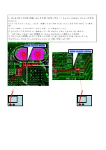
4) Screen ratio problem
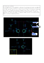
If a strange ratio in 4:3 and 16:9 is detected, the voltage of TV scart pin number 8
is below 9V. In case of around 7V, screen will be shown with 16:9 ratio. In case of
over 10V, the ratio will be 4:3. If there is still a fault on screen after adjusting
screen ratio, it means the resistance of R595 on the circuit is not 1K. If the
voltage is normal but the voltage switch does not operate properly, it means that
Q593 TR is not operating normally. In addition, Q592 can affect the problem because
Q592 is a TV/sat transferring switch .

16:9= 6V
 4:3=11.3V

16:9-High 3.3V

4:3-Low 0V

Summary of Contents for SRT8500

Page 1: ...service manual DTT1609 ...

Page 2: ...ROUBLESOOTHING 3 SCHEMATIC COMPONENT LAYOUT AND BOM OF MAIN BOARD 3 1 SCHEMATIC OF MAIN BOARD 3 3 BOM OF MAIN BOARD 1 1 SHORT TEST 1 MAIN BOARD TROUBLE SHOOTING GUIDE 1 2 POWER 1 3 MAIN CLOCK 1 4 CVBS 1 5 RGB 2 2 COMPONENT LAYOUT OF POWER SUPPLY 2 SCHEMATIC COMPONENT LAYOUT AND BOM OF POWER SUPPLY ...

Page 3: ...DTT1609 Here are the procedures you can refer to whenever terrestrial receivers do not operate properly You can check problems and repair the units on the basic level according to the following procedures Main Board 1 2 3 5 4 7 6 8 9 10 ...

Page 4: ...heck POSITIVE VOLTAGE and also check whether SHORT between GROUND s and PIN SHORT for TUNER are detected or not 2 Checking POWER 12V SCART 5V ANTENNA_POWER IR VIDEO BUFFER HDMI USB 3 3V TUNER FLASH CPU 2 5V DEMOD 1 5V DDR3 CPU 1 3V CPU DEMOD 1 ...

Page 5: ...1 5V 12V 5V For HDMI 6 3V3 For Tuner ...

Page 6: ...2 3V3 For Cpu 10 3V3 1V5 For Cpu 1V5 For DDR3 3 1V3 For Cpu 2 ...

Page 7: ...10 2V5 For DEMOD 5 1V3 For DEMOD 5V For USB 8 5V For Video Buffer 5V For Audio ...

Page 8: ...PU If the 24MHz is unstable Check Y401 is damaged or not If you are firm belief of damage for the device then replace the device And then check that 800MHz is being supplied to DDR3 with RESET If the clock 800MHz on Pin J7 K7 of U401 is not generated from inside of the chip Please check the soldering state of U401 U402 and U403 MAIN CLOCK 24MHz DDR3 CLOCK 800MHz ...

Page 9: ...DDR3 CLOCK 800Mhz MAIN CLOCK ...

Page 10: ...AIN CPU or SCART In case of no MPEG display There can be a variety of reasons for the case Check first that CHANNEL of TP SIGNAL is locked properly After this signal input to the resistor connected to MAIN CPU is done normally A V DATA comes out from MAIN CPU and flows into MPEG CHIP MAIN CPU If there is no problem to here it is thought that MAIN CPU and channel are operating without any fault In ...

Page 11: ...VIDEO SIGNAL If wave form is not like this picture check that wave form output is normal from each terminal ...

Page 12: ...hat ADAC_L U201 PIN2 ADAC_R U201 PIN9 signals have normal inputting and outputting from MAIN CPU The signal is linked to SCART 5 In case of no MPEG and no OSD at the same time Check that 1Vp_p 0 7Vp_p for RGB comes out normally from VIDEO PART CVBS of MAIN CPU BLUE GREEN RED CVBS ...

Page 13: ......

Page 14: ...first if TR on LNB has stopped and then in case that STAND BY mode resulted from wrong software down load a proper software There is a TR s as a switching role on the LNB bundle 5V comes out normally from Q751 If voltage is not enough or steady check if the voltage is impressed properly from Q751 POWER SWITCH ...

Page 15: ... In case of no screen display or different color displayed it also mainly results from the Y401 problem Additionally in case that the screen display works but is with one color only for example blue green or red it mainly results from software fault possiblely detected only on RGB TV RGB Circuit RED GREEN BLUE ...

Page 16: ...Red signal input Blue signal input Green signal input ...

Page 17: ...in LNB Voltage check if the voltage is impressed well into TUNER bundle and if data flow out properly If every condition is satisfied TUNER itself can be considered to be defective In occasion precise inspection should be done in case that there is SHORT between pins fault rarely made by a worker ...

Page 18: ...V the ratio will be 4 3 If there is still a fault on screen after adjusting screen ratio it means the resistance of R595 on the circuit is not 1K If the voltage is normal but the voltage switch does not operate properly it means that Q593 TR is not operating normally In addition Q592 can affect the problem because Q592 is a TV sat transferring switch 16 9 6V 4 3 11 3V 16 9 High 3 3V 4 3 Low 0V ...

Page 19: ......

Page 20: ...2 SCHEMATIC COMPONENT LAYOUT AND BOM OF POWER SUPPLY 2 1 SCHEMATIC OF POWER SUPPLY ...

Page 21: ...2 2 COMPONENT LAYOUT OF POWER SUPPLY 3 SCHEMATIC COMPONENT LAYOUT AND BOM OF MAIN BOARD 3 1 SCHEMATIC OF MAIN BOARD ...

Page 22: ...ATE PCB P N SCH P N DESCRIPTION DOC NO SIGN SIGN SIGN SIGN MODEL NO A Shenzhen Jiuzhou Electric CO LD PAGE DESCRIPTION SIZE Version History V1 0 2011 07 24 Created BLOCK DIAGRAM POWER BLOCK MSD5043 V60 TUNER RCA Video buffer Audio OP SCART ESD HDMI1 3 ESD USB DDR3 Serial FLASH Front pannel POWER LOW IF I2C AGC LMI L R CVBS Y PB PR SPI IR 5V 2A T2 DEMOD TS I2C MSB1230 128MB 4MB Nand FLASH 128MB EEP...

Page 23: ...THIS THIS DOCUMENT IS THE PROPERTY OF Shenzhen Electric CO LD DOC REV PROJECT CODE SHEET DRAWN BY CHECKED BY APPROVED BY DESIGNED BY DATE DATE DATE DATE PCB P N SCH P N DESCRIPTION DOC NO SIGN SIGN SIGN SIGN MODEL NO A Shenzhen Jiuzhou Electric CO LD PAGE DESCRIPTION SIZE GPIO MAPPING TV AV USB Front panel ANT_OVERLOAD TUNER USB_OCD PD_CTRL SCART FLASH_WP MUTE_CTRL TUNER SAR1 PD_CTRL PM_GPIO8 RGB ...

Page 24: ...A9 K1 DDR3_RESET K2 DDR3_A7 K4 DDR3_A5 L2 DDR3_BA0 L4 DDR3_A3 M4 DDR3_WEZ M1 DDR3_CASZ M5 DDR3_ODT M3 DDR3_RASZ N4 DDR3_DQ4 P5 DDR3_DQ2 N5 DDR3_DQ6 P4 DDR3_DQ0 N2 DDR3_DQM1 P2 DDR3_DQ13 P3 DDR3_DQ11 R1 DDR3_DQ15 R3 DDR3_DQ9 T4 DDR3_DQS0 T5 DDR3_DQSB0 T2 DDR3_DQS1 T3 DDR3_DQSB1 U3 DDR3_DQ12 V2 DDR3_DQ8 V3 DDR3_DQ14 W1 DDR3_DQ10 Y1 DDR3_DQM0 U5 DDR3_DQ3 V5 DDR3_DQ5 U4 DDR3_DQ1 V4 DDR3_DQ7 Y2 DDR3_MC...

Page 25: ...ND G9 GND G10 GND G11 GND G12 GND G13 GND G14 GND G15 GND G16 GND G17 GND G19 GND H4 GND H5 GND H6 GND H7 GND H8 GND H9 GND H10 GND H11 GND H12 GND H13 GND H14 GND H15 GND H16 GND H17 GND J5 GND J6 GND J7 GND J8 GND J9 GND J10 GND J11 GND J12 GND J13 GND J14 GND J15 GND J16 GND J17 GND J18 GND K3 GND K5 GND K6 GND K7 GND K8 GND K9 GND K10 GND K11 GND K12 GND K13 GND K14 GND K15 GND K16 GND K17 GND...

Page 26: ...Q G9 VSSQ B2 VDD D9 VDD G7 VDD K2 VDD K8 VDD N1 VDD N9 VDD R1 VDD R9 VDD A9 VSS E1 VSS G8 VSS J2 VSS J8 VSS M1 VSS M9 VSS P1 VSS P9 VSS T1 VSS T9 VSS J1 NC1 J9 NC2 L1 NC3 L9 NC4 M7 NC5 T3 A13 T7 NC7 B3 VSS U402 DDR3_2Gbit_1600 R450 240R 1 D5 CLE H4 I O0 C3 WP C8 R B C6 CE D4 RE C7 WE K3 VSS J6 VDD H8 VDD C5 VSS C4 ALE J4 I O1 K4 I O2 K5 I O3 K6 I O4 J7 I O5 K7 I O6 J8 I O7 K8 VSS U406 Nand 128M C4...

Page 27: ...4 GND 5 SHIELD J501 USB A Female 2 0 pitch R512 ESD R511 ESD R501 5R1 R502 5R1 1 T3 T 1 T4 T C512 8 2P C511 8 2P 2 3 4 5 6 8 7 9 X2 2 3 4 5 6 8 7 9 X4 2 3 4 5 6 8 7 9 X1 1 X5 HOLE 1 MARK2 MARK 1 MARK3 MARK 1 MARK1 MARK 1 MARK4 MARK 1 MARK5 MARK F601 FUSH SMD1210 B E C Q601 BC857 R619 1K R617 NC 0R R618 220R 1 VCC 2 RST 3 CLK 4 C4 9 SC_DET1 10 SC_DET2 8 C8 7 IO 6 VPP 5 GND J502 ICA 619 R567 18K C56...

Page 28: ...SHIELD J801 C254 100P R597 150R R598 10K B E C Q594 3904 R599 1K R560 150R R593 10K B E C Q592 3904 R594 1 5K 0603 R595 1 5K 0603 B E C Q593 3904 R596 10K R591 10K R592 10K 1 IN1 2 IN2 3 IN3 4 VCC 8 OUT1 7 OUT2 6 OUT3 5 GND U302 NCS2553 R312 75R R315 75R R317 75R C324 47P L304 600R C322 47P L305 600R C323 47P L306 600R C309 104 C308 104 L301 FB 60R 0603 CE301 100uf 16v R301 NC 1 IN1 2 IN2 3 IN3 4 ...

Page 29: ...LL_TS SDR 49 GPIO 0 50 VDD33 51 VDD 52 VSS 53 VDD33 54 I2CM_SCL 55 I2CM_SDA 56 RF_AGC 57 IF_AGC 58 VSS 59 VDD 60 VDD33 61 TESTPIN 62 I2CS_SCL 63 I2CS_SDA 64 GPIO 3 U701 MSB1230 C706 NC R708 NC 10K C704 104 L707 FB 60R 300mA 0603 C709 NC R706 2K R714 4K7 R713 22R L706 FB 60R 300mA 0603 R709 NC 10K C737 104 L708 FB 60R 300mA 0603 C703 104 R707 NC 10K C721 104 C707 NC C705 104 R705 2K C734 104 L705 F...

Page 30: ...56 75R R660 510R R652 49 9R C656 103 1 TX 2 TX 3 RX 4 TXCT 5 RXCT 6 RX 7 NC 8 CH_GND 11 GND 12 GND 9 10 13 LED0 14 LED0 15 LED1 16 LED1 J651 98LEDC03 1X1 TP RJ45 C672 104 C668 10uF 0805 R672 NC C667 104 R683 33R R674 10K R675 1 5K R665 100R R677 0R C663 104 R666 100R C662 33P R684 1M R676 300K C664 30P R667 100R R679 0R C666 10uF 0805 R681 0R 12 MDIO 13 MDC 7 RXD1 MODE1 8 RXD0 MODE0 14 NINT REFCLK...

Page 31: ...2 3 4 5 6 CON121 6PIN 2 0MM R125 4K7 1 BS 2 IN 3 SW 4 GND 5 FB 6 COMP 7 EN 8 SS U131 MP1482 C131 10uF 0805 C132 104 R134 10K C134 47nF C133 10nF L132 10uH 2A DIP 5 8 R132 20K 1 R133 47K 1 C135 10uF 0805 CE132 220uf 16v L131 FB120R 0805 R186 10K R185 10K B E C Q184 3904 B E C Q183 3904 R188 1K R187 10K C146 104 L142 4 7uH 1A L181 NC FB120R 0805 R154 100R C154 104 R135 100R C136 104 CE107 100uf 16v ...

Page 32: ... DATE APP BY 1 B C A B C D 4 6 5 Xuewei 2011 12 19 11 11 OF A2 V1 1 AC DC 快速放电电路 Fuse 50V 2 1 3 4 5 6 7 8 9 10 T901 KB1025 15582 1 2 4 3 U902 LTV 817 C 4 D 8 S 7 5 3 2 BP 1 EN 6 U901 TNY176DG F902 T1AL 250V D912 IN4007 D913 IN4007 D911 IN4007 D910 IN4007 RT901 10D 9 1 2 3 U903 TL431 C910 10uF 400V C911 22uf 400v C913 472 1KV R921 200K 1206 D916 1N4007 R919 100K 0603 C912 10uf 50v L902 4 7uH 2A C91...

Page 33: ......

Page 34: ......

Page 35: ......

Page 36: ......

Page 37: ...005 14 3 C216 C218 C409 C CERAMIC CHIP 2 2nF 10 50V X7R TP 1005 15 6 C133 C445 C448 C458 C465 C476 C CERAMIC CHIP 10nF 10 50V X7R TP 1005 16 1 C710 C CERAMIC CHIP 22nF 10 25V X7R TP 1005 17 1 C134 C CERAMIC CHIP 47nF 10 16V X7R TP 1005 18 86 C105 C106 C111 C113 C114 C132 C136 C145 C146 C154 C155 C174 C175 C181 C201 C251 C252 C308 C309 C412 C421 C422 C423 C424 C427 C428 C429 C430 C431 C434 C435 C43...

Page 38: ... R436 R569 R599 R615 R619 R716 R752 R754 R756 R CHIP 1K ohm 5 1 16W DA TP 1005 38 4 R611 R612 R705 R706 R CHIP 2K ohm 5 1 16W DA TP 1005 39 9 R103 R104 R125 R127 R232 R426 R427 R714 R715 R CHIP 4 7K ohm 5 1 16W DA TP 1005 40 2 R221 R222 R CHIP 5 1K ohm 5 1 16W DA TP 1005 40 43 R121 R122 R123 R124 R134 R182 R183 R185 R186 R187 R227 R228 R408 R410 R414 R415 R505 R506 R508 R521 R522 R523 R524 R525 R5...

Page 39: ...IER IN4007 DO 214AC SMT 78 1 D918 Diode Zener ZMM18 18V LL 34 SMD 79 1 D920 FAST RECOVERY RECTIFIER FR104 DO 214AC SMT 80 1 Q123 N CHANNEL ENHANCEMENT MODE FIELD EFFECT TRANSISTOR BS870 7 F SOT 23 81 11 Q121 Q122 Q182 Q183 Q184 Q191 Q251 Q592 Q593 Q594 Q753 TR SMALL SIGNAL KST3904 MTF MMBT3904LT1 LMBT3904LTIG NPN 60V 40V 200mA 350mW SOT 23 82 3 Q401 Q601 Q752 TR SMALL SIGNAL KST3906 MTF MMBT3906LT...

Page 40: ...NG CUT TYPE 11 1 CY902 Y1 CAP 1000PF 400V 20 BARREL 8 10 25 12 1 C913 4 7nF 1KV Y5U 10 13 1 C915 C Aluminum 1000UF 16V 20 BARREL10 16 5 高频低阻 供应商 金富康 14 4 D910 D911 D912 D913 DIODE RECTIFIER 1N4007ID 1000V 1A DO 41 15 2 D917 D919 SCHOTTKY BARRIER RECTIFIERS 1N5822 3 0A TO 27 16 1 U903 Regulator MOSFET ZL431AZ ATRE1 precision is 0 4 TO 92 17 1 U902 光耦 LTV 817 CN 200 400 DIP 4 18 1 U901 Power switch ...

Page 41: ...34 1 FOR D191 LED SUPPORT 12MM 35 1 J501 USB A 04 USB插座 侧弯90度 36 1 SW101 SWITCH PUSH 6X6X2DH5 H 1 5mm 37 TUNER2 DVB T2 T TUNER FH RT232A4 9 2PINS 立式 38 1 FOR U401 Heat SINK 25 25 20 white ...

Page 42: ...en your STB works or even NO SIGNAL please change the crystal in the TUNER and if that fails change the Tuner module directly 1 Testing the chip and the DEMOD s crystal frequency Y401 Y701 with a frequency spectrograph to make sure it s within 20PPM 480HZ ...

Page 43: ...3 If the fuse blew out please change the F902 and check the D910 D911 D912 D913 to see if they are burnout ...

Reviews: