background image

13

400 MHz CPU, 4.0 MB E-Cache

UltraSPARC

-II CPU Module

SME5224AUPA-400

Advanced Version

July 1999

Sun Microsystems, Inc

UPA Data Bus SPICE Model

A typical circuit for the UPA data bus and ECC signals is illustrated in Figure 4:.

Figure 4. Module System Loading: Example for UPA_DATA, UPA_ECC

3.1 nH

1.0 pF

Edge Connector

UDB-II Driver

Trace 1

0.5 nH

2 nH

50

via 0.6 pF

7 pF

Trace 2

XB1 BGA Package Loading

3.1 nH

Edge Connector

Trace 3

0.5 nH

2 nH

50

via 0.6 pF

7 pF

UDB-II of Second Module

Package Loading

Trace 4

Measure point for XB1

Measure point for CPU

Worst Case: Z

0

= 60

, T

P

= 180 ps/inch, Trace 1 Length = 4.4”, Trace 2 Length = 0.6”, Trace 3 Length

= 1.2”, Trace 4 Length = 4.4”

Best Case: Z

0

= 50

, T

P

= 160 ps/inch, Trace 1 Length = 2.2”, Trace 2 Length = 0.2”, Trace 3 Length

= 0.2”, Trace 4 Length = 2.2”

1.0 pF

1.0 pF 1.0 pF

Summary of Contents for SME5224AUPA-400

Page 1: ...grade and field support Module Features Module Benefits Ease of System Design Small form factor board with integrated external cache and UPA interface JTAG boundary scan and performance instrumentation PCB provides a multi power plane bypass reducing systemboard design requirements Performance High performance UltraSPARC CPU at 400MHz Four megabytes of external cache using high speed register latc...

Page 2: ...ance Thirty two 64 bit integer registers Allows applications to store data locally in the register files Superscalar Superpipelined Allows for multiple integer and floating point execution units leading to higher application performance High performance memory interconnect Alleviating the bottleneck of bandwidth to main memory Built in Multiprocessing Capability Delivering scalability at the syste...

Page 3: ...U Each UDB II has a 64 bit interface plus eight parity bits on the CPU side and a 64 bit interface plus eight error correction code ECC bits on the system side The CPU side of the UDB II is clocked with the same clock delivered to UltraSPARC II 1 2 of the CPU pipe line frequency EXTERNAL CACHE DESCRIPTION The external cache is connected to the E cache data bus Nine SRAM chips are used to implement...

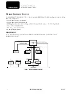
Page 4: ... data SRAMs and one 128K X 36 Tag SRAM Clock Buffer MC100LVE210 DC DC regulator 2 6V to 1 9V Module Airflow Shroud Block Diagram The module block diagram for the UltraSPARC II 400 MHz CPU 4 Mbyte E cache module is illustrated in Figure 1 Figure 1 Module Block Diagram Tag SRAM 128K x 36 SRAM 256K x 18 Tag SRAM ADDR 17 0 Control Tag SRAM DATA 24 0 UltraSPARC II CPU UDB II UDB II SRAM ADDR 19 0 Contr...

Page 5: ...or and are represented on page 24 and page 25 UPA Interconnect The UltraSPARC II 400 MHz CPU 4 0 Mbyte module SME5224AUPA 400 supports full master and slave functionality with a 128 bit data bus and a 16 bit error correction code ECC All signals that interface with the system are compatible with LVTTL levels The clock inputs at the module connector CPU_CLK UPA_CLK0 and UPA_CLK1 are differential lo...

Page 6: ...tion specific means in the system System firmware Open Boot Prom uses UPA_CONFIG_REG 42 39 for generating correct clocks to the CPU module and the UPA system ASICs These bits are hardwired on the module and are known at MCAP 3 0 at the UltraSPARC II pins The 4 bit MCAP value for this module is 0111b Module Power Two types of power are required for this module VDD at 3 3V and VDD_CORE at 2 6V The V...

Page 7: ...ive high UPA_S_REPLY 4 0 I UltraSPARC II system reply packet driven by system controller to the UPA port Synchronous to UPA_CLK Active high UPA_S_REPLY 4 is a no connect UPA_DATA_STALL I Driven by system controller to indicate whether there is a data stall Active high UPA_P_REPLY 4 0 O UltraSPARC II system reply packet driven by the UltraSPARC II to the system Synchronous to UPA_CLK Active high UP...

Page 8: ...n Interface Signal Type Name and Function UPA_RESET_L I Driven by the system controller for the POR power on resets and the fatal system reset Asserted asynchronously Deasserted synchronous to UPA_CLK Active low UPA_XIR_L I Driven to signal externally initiated reset XIR Actually acts like a non maskable interrupt Synchronous to UPA_CLK Active low asserted for one clock cycle Miscellaneous Signals...

Page 9: ...ider clock buffers and terminators The buffers fan out the LVPECL clocks to the many UPA devices the module cross bar data switches system controller FFB and the system I O bridge The LVPECL clock trace pairs are routed source to destination Each net is terminated at the destination Most destinations are to single devices The PCB traces for the LVPECL clocks are balanced to provide a high degree o...

Page 10: ...ck frequency presented at its clock pin So for a 400 MHz core CPU clock frequency the CPU_CLK signal is 200 MHz Therefore for the CPU actions will appear to occur at both tran sitions of the input CPU_CLK CLOCK TRACE DELAYS The LVPECL propagation time is constant for all clock signals so all balancing is based on length rather than time All LVPECL traces are striplines dielectric and power planes ...

Page 11: ...DD_CORE for 30 ms or less provided that the current is limited to twice thew maximum CPU rating Supply voltage range for CPU core 0 to 3 0 V VI Input voltage range 3 3 Unless otherwise noted all voltages are with respect to the VSS ground 0 5 to VDD 0 5 V VO Output voltage range 0 5 to VDD 0 5 V IIK Input clamp current 20 mA IOK Output clamp current 50 mA IOL Current into any output in the low sta...

Page 12: ...w level output voltage VDD Min IOL Max 0 4 V IDD Supply current for VDD 2 3 2 The supply current for the VDD includes the supply current for the CPU UDB II and the SRAMs 3 The typical DC current values represent the current drawn at nominal voltage with a typical busy computing load Variations in the device computing load and system implementation affect the actual current The maximum DC current v...

Page 13: ... pF Edge Connector UDB II Driver Trace 1 0 5 nH 2 nH 50 Ω via 0 6 pF 7 pF Trace 2 XB1 BGA Package Loading 3 1 nH Edge Connector Trace 3 0 5 nH 2 nH 50 Ω via 0 6 pF 7 pF UDB II of Second Module Package Loading Trace 4 Measure point for XB1 Measure point for CPU Worst Case Z0 60Ω TP 180 ps inch Trace 1 Length 4 4 Trace 2 Length 0 6 Trace 3 Length 1 2 Trace 4 Length 4 4 Best Case Z0 50Ω TP 160 ps inc...

Page 14: ...the effective trace length of CPU_CLK on the module 18 inches including the module connector Clock Buffers The Clock buffer on the systemboard and the clock buffer on the module are assumed to have similar delays The clock buffers have a 600 ps delay Timing References The setup hold and clock to output timing specifications are referenced at the module connector for the sig nal and at the system U...

Page 15: ...e Specifications Symbol Clock to Out Signals and Output Hold Signals Waveforms 400 MHz CPU 100 MHz UPA Unit Min Max tP Clock to Out UPA_DATA 127 0 2 3 8 ns UPA_ADDR 35 0 UPA_ADDR_VALID UPA_P_REPLY 4 0 UPA_REQ_OUT 2 3 1 ns UPA_ECC 15 0 2 3 8 ns tOH Output Hold UPA_DATA 127 0 2 1 1 ns UPA_ADDR 35 0 UPA_ADDR_VALID UPA_P_REPLY 4 0 2 1 1 ns UPA_ECC 15 0 2 1 1 ns Setup and Hold Time Specifications Symbo...

Page 16: ... 8 and Figure 9 Figure 6 CPU Module Components Figure 7 CPU Module Component Dimensions Module Ejectors CPU Voltage Regulator Heat Sink Thermistor Location RT0201 UDB Heat Sinks Front SRAM Heat Sinks 0 179 4 55 0 315 8 00 4 250 107 95 3 680 93 47 0 570 14 48 0 535 13 59 0 540 13 72 6 250 158 75 3 213 81 61 Pin 328 Pin 1 2 551 64 79 0 112 2 86 0 174 4 41 5 890 149 61 200 5 08 Dimensions inches mill...

Page 17: ...OTE A minimum backside clearance is required for airflow cooling of the backside heatsink Module Shroud Bidirectional Airflow Backside SRAM Heat sink Bidirectional Airflow 1 318 33 48 Maximum Provide Minimum 0 079 2 00 Backside Clearance 0 298 7 57 Maximum Maximum Card Guide Depth 0 087 2 201 Provide Minimum Frontside Clearance 0 079 2 00 0 062 0 008 1 57 0 20 Dimensions inches millimeters ...

Page 18: ...the entire operating range of the system This includes both the compute load and the environmental conditions for the system If measuring the case temperature is prob lematic then measure the heatsink temperature and calculate the junction temperature Both approaches for calculating junction temperature are explained in this section Irrespective of which method is used accurate measurement is requ...

Page 19: ...ch is to embed a thermocouple in a cavity drilled in the heatsink base An alternative approach is to place the thermocouple between the fins pins of the heat sink insulated from the airflow and in contact with the base plate of the heatsink Ta Module ambient air temperature see page 20 The air temperature as it approaches the heatsink Pd Typical power dissipation of the CPU 19 0 W The worst case c...

Page 20: ...mance of the fan that is supplying the airflow Calculating the airflow velocity is difficult It is subject to the interpretation of the term free stream Note The Airflow Cooling Estimate method is an estimate Use it solely when an approximate value suffices Accuracy can only be assured using the Case Temperature measuring method or the Heatsink Temperature measuring method Apply these methods to i...

Page 21: ... Pd x θjc Note Testing is done with the worst case power draw software loading and ambient air temperature There is good tracking between the case temperature and the heatsink temperature Heatsink Temperature Measuring Method Measuring the heatsink temperature is sometimes easier than measuring the case temperature This method provides accurate results for most designs If the heatsink temperature ...

Page 22: ...module except the clock buffer AC Characteristics JTAG Timing Symbol Parameter Signals Conditions 400 MHz CPU 10 MHz TCK Units Min Typ Max tW TRST Test reset pulse width TRST 1 1 TRST is an asynchronous reset ns tSU TDI Input setup time to TCK TDI 3 ns tSU TMS Input setup time to TCK TMS 4 ns tH TDI Input hold time to TCK TDI 1 5 ns tH TMS Input hold time to TCK TMS 1 5 ns tPD TDO Output delay fro...

Page 23: ...un Microsystems Inc JTAG IEEE 1149 1 TIMING Figure 10 Voltage Waveforms Setup and Hold Times Data Input tH 1 5V VIH VIL Clock tSU 2 0V VIH VIL 1 5V Figure 11 Voltage Waveforms Propagation Delay Times Clock tPD In Phase Output Out of Phase Output 2 0V 2 0V VIH VIL VOH VOL VOH VOL tOH tPD tOH 0 8V 0 8V ...

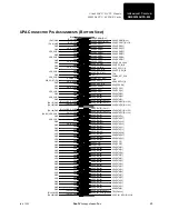
Page 24: ...D VDD GND VDD GND GND GND VDD GND GND GND GND VDD GND VDD UPA_ADDR 5 UPA_ADDR 7 UPA_ADDR 17 UPA_ADDR 19 UPA_ADDR 21 UPA_ADDR 23 UPA_ADDR 33 UPA_RATIO UPA_P_REPLY 0 UPA_P_REPLY 2 UPA_CLK0_POS TDI TEMP_SENSE_NEG UPA_S_REPLY 0 UPA_S_REPLY 2 UPA_ECC 11 UPA_ECC 9 UPA_DATA 87 UPA_DATA 85 UPA_DATA 83 Pin 136 UPA_DATA 81 Pin 142 UPA_DATA 71 Pin 148 UPA_DATA 69 Pin 145 UPA_DATA 70 Pin 154 UPA_DATA 67 Pin 1...

Page 25: ...ND GND VDD GND VDD GND GND GND VDD GND GND GND GND VDD GND VDD UPA_ADDR 13 UPA_ADDR 15 UPA_ADDR 25 UPA_ADDR 27 UPA_ADDR 29 UPA_ADDR 31 UPA_ADDR_VALID UPA_REQ_IN 0 UPA_P_REPLY 3 UPA_SC_REQ_IN TCK POWER_SET_POS TMS UPA_S_REPLY 3 UPA_SPEED 2 UPA_ECC 15 UPA_ECC 13 UPA_DATA 95 UPA_DATA 93 UPA_DATA 91 UPA_DATA 89 Pin 138 UPA_DATA 79 Pin 144 UPA_DATA 77 Pin 150 UPA_DATA 78 Pin 147 UPA_DATA 75 Pin 156 UPA...

Page 26: ... cause unseen damage to the solder connections Always handle modules and other electronic devices in an ESD controlled environment STORAGE AND SHIPPING SPECIFICATION Parameter Conditions Value Unit Min Typ Max Temperature Ambient 40 90 C Temperature ramp Ambient 10 C min Shock shipping single module package Drop height on to any edge corner or side of shipping box 21 inches Shock shipping multi mo...

Page 27: ...ICs DOCUMENT REVISION HISTORY Date Document No Change July 1999 805 4835 05 This module is designed using the the UltraSPARC II 400 MHz CPU revision 3 x See page 9 Module Clocks for changes effecting this version of the module May 1999 805 6390 04 Re organization of the datasheet and update of specifications March 1999 805 6390 03 Preliminary Version New section concerning the System Timing and Th...

Page 28: ...un Microsystems the Sun Logo Ultra and VIS are trademarks or registered trademarks of Sun Microsystems Inc in the United States and other countries All SPARC trademarks are used under license and are trademarks or registered trademarks of SPARC International Inc in the United States and other countries Products bearing SPARC trademarks are based upon an architecture developed by Sun Microsystems I...

Page 29: ...grade and field support Module Features Module Benefits Ease of System Design Small form factor board with integrated external cache and UPA interface JTAG boundary scan and performance instrumentation PCB provides a multi power plane bypass reducing systemboard design requirements Performance High performance UltraSPARC CPU at 400MHz Four megabytes of external cache using high speed register latc...

Page 30: ...ance Thirty two 64 bit integer registers Allows applications to store data locally in the register files Superscalar Superpipelined Allows for multiple integer and floating point execution units leading to higher application performance High performance memory interconnect Alleviating the bottleneck of bandwidth to main memory Built in Multiprocessing Capability Delivering scalability at the syste...

Page 31: ...U Each UDB II has a 64 bit interface plus eight parity bits on the CPU side and a 64 bit interface plus eight error correction code ECC bits on the system side The CPU side of the UDB II is clocked with the same clock delivered to UltraSPARC II 1 2 of the CPU pipe line frequency EXTERNAL CACHE DESCRIPTION The external cache is connected to the E cache data bus Nine SRAM chips are used to implement...

Page 32: ... data SRAMs and one 128K X 36 Tag SRAM Clock Buffer MC100LVE210 DC DC regulator 2 6V to 1 9V Module Airflow Shroud Block Diagram The module block diagram for the UltraSPARC II 400 MHz CPU 4 Mbyte E cache module is illustrated in Figure 1 Figure 1 Module Block Diagram Tag SRAM 128K x 36 SRAM 256K x 18 Tag SRAM ADDR 17 0 Control Tag SRAM DATA 24 0 UltraSPARC II CPU UDB II UDB II SRAM ADDR 19 0 Contr...

Page 33: ...or and are represented on page 24 and page 25 UPA Interconnect The UltraSPARC II 400 MHz CPU 4 0 Mbyte module SME5224AUPA 400 supports full master and slave functionality with a 128 bit data bus and a 16 bit error correction code ECC All signals that interface with the system are compatible with LVTTL levels The clock inputs at the module connector CPU_CLK UPA_CLK0 and UPA_CLK1 are differential lo...

Page 34: ...tion specific means in the system System firmware Open Boot Prom uses UPA_CONFIG_REG 42 39 for generating correct clocks to the CPU module and the UPA system ASICs These bits are hardwired on the module and are known at MCAP 3 0 at the UltraSPARC II pins The 4 bit MCAP value for this module is 0111b Module Power Two types of power are required for this module VDD at 3 3V and VDD_CORE at 2 6V The V...

Page 35: ...ive high UPA_S_REPLY 4 0 I UltraSPARC II system reply packet driven by system controller to the UPA port Synchronous to UPA_CLK Active high UPA_S_REPLY 4 is a no connect UPA_DATA_STALL I Driven by system controller to indicate whether there is a data stall Active high UPA_P_REPLY 4 0 O UltraSPARC II system reply packet driven by the UltraSPARC II to the system Synchronous to UPA_CLK Active high UP...

Page 36: ...n Interface Signal Type Name and Function UPA_RESET_L I Driven by the system controller for the POR power on resets and the fatal system reset Asserted asynchronously Deasserted synchronous to UPA_CLK Active low UPA_XIR_L I Driven to signal externally initiated reset XIR Actually acts like a non maskable interrupt Synchronous to UPA_CLK Active low asserted for one clock cycle Miscellaneous Signals...

Page 37: ...ider clock buffers and terminators The buffers fan out the LVPECL clocks to the many UPA devices the module cross bar data switches system controller FFB and the system I O bridge The LVPECL clock trace pairs are routed source to destination Each net is terminated at the destination Most destinations are to single devices The PCB traces for the LVPECL clocks are balanced to provide a high degree o...

Page 38: ...ck frequency presented at its clock pin So for a 400 MHz core CPU clock frequency the CPU_CLK signal is 200 MHz Therefore for the CPU actions will appear to occur at both tran sitions of the input CPU_CLK CLOCK TRACE DELAYS The LVPECL propagation time is constant for all clock signals so all balancing is based on length rather than time All LVPECL traces are striplines dielectric and power planes ...

Page 39: ...DD_CORE for 30 ms or less provided that the current is limited to twice thew maximum CPU rating Supply voltage range for CPU core 0 to 3 0 V VI Input voltage range 3 3 Unless otherwise noted all voltages are with respect to the VSS ground 0 5 to VDD 0 5 V VO Output voltage range 0 5 to VDD 0 5 V IIK Input clamp current 20 mA IOK Output clamp current 50 mA IOL Current into any output in the low sta...

Page 40: ...w level output voltage VDD Min IOL Max 0 4 V IDD Supply current for VDD 2 3 2 The supply current for the VDD includes the supply current for the CPU UDB II and the SRAMs 3 The typical DC current values represent the current drawn at nominal voltage with a typical busy computing load Variations in the device computing load and system implementation affect the actual current The maximum DC current v...

Page 41: ... pF Edge Connector UDB II Driver Trace 1 0 5 nH 2 nH 50 Ω via 0 6 pF 7 pF Trace 2 XB1 BGA Package Loading 3 1 nH Edge Connector Trace 3 0 5 nH 2 nH 50 Ω via 0 6 pF 7 pF UDB II of Second Module Package Loading Trace 4 Measure point for XB1 Measure point for CPU Worst Case Z0 60Ω TP 180 ps inch Trace 1 Length 4 4 Trace 2 Length 0 6 Trace 3 Length 1 2 Trace 4 Length 4 4 Best Case Z0 50Ω TP 160 ps inc...

Page 42: ...the effective trace length of CPU_CLK on the module 18 inches including the module connector Clock Buffers The Clock buffer on the systemboard and the clock buffer on the module are assumed to have similar delays The clock buffers have a 600 ps delay Timing References The setup hold and clock to output timing specifications are referenced at the module connector for the sig nal and at the system U...

Page 43: ...e Specifications Symbol Clock to Out Signals and Output Hold Signals Waveforms 400 MHz CPU 100 MHz UPA Unit Min Max tP Clock to Out UPA_DATA 127 0 2 3 8 ns UPA_ADDR 35 0 UPA_ADDR_VALID UPA_P_REPLY 4 0 UPA_REQ_OUT 2 3 1 ns UPA_ECC 15 0 2 3 8 ns tOH Output Hold UPA_DATA 127 0 2 1 1 ns UPA_ADDR 35 0 UPA_ADDR_VALID UPA_P_REPLY 4 0 2 1 1 ns UPA_ECC 15 0 2 1 1 ns Setup and Hold Time Specifications Symbo...

Page 44: ... 8 and Figure 9 Figure 6 CPU Module Components Figure 7 CPU Module Component Dimensions Module Ejectors CPU Voltage Regulator Heat Sink Thermistor Location RT0201 UDB Heat Sinks Front SRAM Heat Sinks 0 179 4 55 0 315 8 00 4 250 107 95 3 680 93 47 0 570 14 48 0 535 13 59 0 540 13 72 6 250 158 75 3 213 81 61 Pin 328 Pin 1 2 551 64 79 0 112 2 86 0 174 4 41 5 890 149 61 200 5 08 Dimensions inches mill...

Page 45: ...OTE A minimum backside clearance is required for airflow cooling of the backside heatsink Module Shroud Bidirectional Airflow Backside SRAM Heat sink Bidirectional Airflow 1 318 33 48 Maximum Provide Minimum 0 079 2 00 Backside Clearance 0 298 7 57 Maximum Maximum Card Guide Depth 0 087 2 201 Provide Minimum Frontside Clearance 0 079 2 00 0 062 0 008 1 57 0 20 Dimensions inches millimeters ...

Page 46: ...the entire operating range of the system This includes both the compute load and the environmental conditions for the system If measuring the case temperature is prob lematic then measure the heatsink temperature and calculate the junction temperature Both approaches for calculating junction temperature are explained in this section Irrespective of which method is used accurate measurement is requ...

Page 47: ...ch is to embed a thermocouple in a cavity drilled in the heatsink base An alternative approach is to place the thermocouple between the fins pins of the heat sink insulated from the airflow and in contact with the base plate of the heatsink Ta Module ambient air temperature see page 20 The air temperature as it approaches the heatsink Pd Typical power dissipation of the CPU 19 0 W The worst case c...

Page 48: ...mance of the fan that is supplying the airflow Calculating the airflow velocity is difficult It is subject to the interpretation of the term free stream Note The Airflow Cooling Estimate method is an estimate Use it solely when an approximate value suffices Accuracy can only be assured using the Case Temperature measuring method or the Heatsink Temperature measuring method Apply these methods to i...

Page 49: ... Pd x θjc Note Testing is done with the worst case power draw software loading and ambient air temperature There is good tracking between the case temperature and the heatsink temperature Heatsink Temperature Measuring Method Measuring the heatsink temperature is sometimes easier than measuring the case temperature This method provides accurate results for most designs If the heatsink temperature ...

Page 50: ...module except the clock buffer AC Characteristics JTAG Timing Symbol Parameter Signals Conditions 400 MHz CPU 10 MHz TCK Units Min Typ Max tW TRST Test reset pulse width TRST 1 1 TRST is an asynchronous reset ns tSU TDI Input setup time to TCK TDI 3 ns tSU TMS Input setup time to TCK TMS 4 ns tH TDI Input hold time to TCK TDI 1 5 ns tH TMS Input hold time to TCK TMS 1 5 ns tPD TDO Output delay fro...

Page 51: ...un Microsystems Inc JTAG IEEE 1149 1 TIMING Figure 10 Voltage Waveforms Setup and Hold Times Data Input tH 1 5V VIH VIL Clock tSU 2 0V VIH VIL 1 5V Figure 11 Voltage Waveforms Propagation Delay Times Clock tPD In Phase Output Out of Phase Output 2 0V 2 0V VIH VIL VOH VOL VOH VOL tOH tPD tOH 0 8V 0 8V ...

Page 52: ...D VDD GND VDD GND GND GND VDD GND GND GND GND VDD GND VDD UPA_ADDR 5 UPA_ADDR 7 UPA_ADDR 17 UPA_ADDR 19 UPA_ADDR 21 UPA_ADDR 23 UPA_ADDR 33 UPA_RATIO UPA_P_REPLY 0 UPA_P_REPLY 2 UPA_CLK0_POS TDI TEMP_SENSE_NEG UPA_S_REPLY 0 UPA_S_REPLY 2 UPA_ECC 11 UPA_ECC 9 UPA_DATA 87 UPA_DATA 85 UPA_DATA 83 Pin 136 UPA_DATA 81 Pin 142 UPA_DATA 71 Pin 148 UPA_DATA 69 Pin 145 UPA_DATA 70 Pin 154 UPA_DATA 67 Pin 1...

Page 53: ...ND GND VDD GND VDD GND GND GND VDD GND GND GND GND VDD GND VDD UPA_ADDR 13 UPA_ADDR 15 UPA_ADDR 25 UPA_ADDR 27 UPA_ADDR 29 UPA_ADDR 31 UPA_ADDR_VALID UPA_REQ_IN 0 UPA_P_REPLY 3 UPA_SC_REQ_IN TCK POWER_SET_POS TMS UPA_S_REPLY 3 UPA_SPEED 2 UPA_ECC 15 UPA_ECC 13 UPA_DATA 95 UPA_DATA 93 UPA_DATA 91 UPA_DATA 89 Pin 138 UPA_DATA 79 Pin 144 UPA_DATA 77 Pin 150 UPA_DATA 78 Pin 147 UPA_DATA 75 Pin 156 UPA...

Page 54: ... cause unseen damage to the solder connections Always handle modules and other electronic devices in an ESD controlled environment STORAGE AND SHIPPING SPECIFICATION Parameter Conditions Value Unit Min Typ Max Temperature Ambient 40 90 C Temperature ramp Ambient 10 C min Shock shipping single module package Drop height on to any edge corner or side of shipping box 21 inches Shock shipping multi mo...

Page 55: ...ICs DOCUMENT REVISION HISTORY Date Document No Change July 1999 805 4835 05 This module is designed using the the UltraSPARC II 400 MHz CPU revision 3 x See page 9 Module Clocks for changes effecting this version of the module May 1999 805 6390 04 Re organization of the datasheet and update of specifications March 1999 805 6390 03 Preliminary Version New section concerning the System Timing and Th...

Page 56: ...un Microsystems the Sun Logo Ultra and VIS are trademarks or registered trademarks of Sun Microsystems Inc in the United States and other countries All SPARC trademarks are used under license and are trademarks or registered trademarks of SPARC International Inc in the United States and other countries Products bearing SPARC trademarks are based upon an architecture developed by Sun Microsystems I...

Reviews: