background image

1-6-7

T7500EA

13. Convergence Adjustment

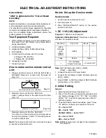
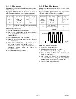
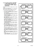
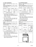
Purpose:

 To obtain proper convergence of red, green

and blue beams.

Symptom of Misadjustment:

 If Convergence Adjust-

ment is incorrect, the edge of white letters may have
color edges.

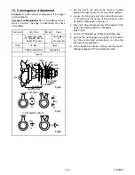
1. Set the unit to the AUX mode which is located

before CH2 then input a Dot or crosshatch pattern.

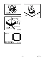
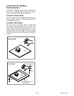
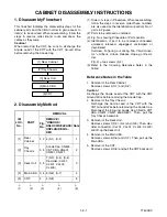
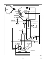
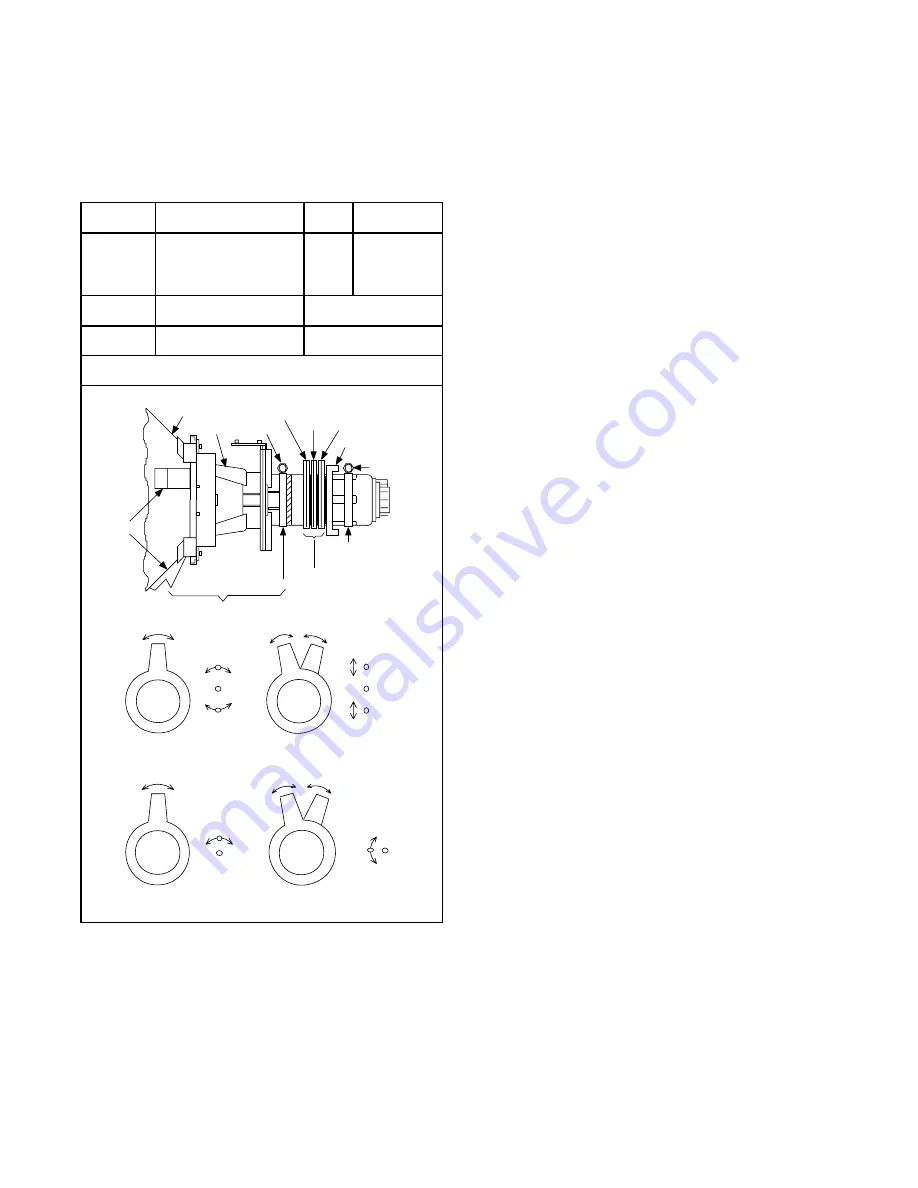
2. Loosen the Ring Lock and align red with blue dots

or Crosshatch at the center of the screen by rotat-
ing (RB) C.P. Magnets. (See Fig. 7.)

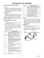
3. Align red / blue with green dots at the center of the

screen by rotating (RB-G) C.P. Magnet. 
(See Fig. 8.)

4. Fix the C.P. Magnets by tightening the Ring Lock.

5. Remove the DY Wedges and slightly tilt the Deflec-

tion Yoke horizontally and vertically to obtain the
best overall convergence.

6. Fix the Deflection Yoke by carefully inserting the DY

Wedges between CRT and Deflection Yoke.

Test point

Adj. Point

Mode

Input

---

C.P. Magnet (RB),

C.P. Magnet (RB-G),

Deflection Yoke

---

Dot Pattern 

or 

Crosshatch

Tape

M. EQ.

Spec.

---

Pattern Generator

See below.

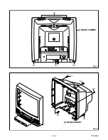
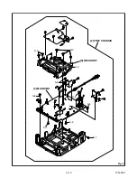
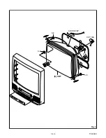
Figure

DY WEDGE

DEFLECTION YOKE

C.P. MAGNET

RING LOCK

SCREW

SCREW

RB-G

RB

PURITY

CRT

COIL

COIL CLAMPER

C.P. MAGNET 
CLAMPER

Fig. 6

Fig. 7

Fig. 8

B

G

R

R

G

B

 C.P. MAGNET (RB)

RB

G

RB

G

 C.P. MAGNET (RB-G)

Summary of Contents for 6319CE

Page 1: ...ain Section I Specifications I Preparation for Servicing I Adjustment Procedures I Schematic Diagrams I CBA s I Exploded Views I Parts List When servicing the deck mechanism refer to MK12 5 Deck Mecha...

Page 2: ...njury to service personnel The possibility exists that improper ser vice methods may damage the equipment It also is important to understand that these CAUTIONS and NOTICES ARE NOT EXHAUSTIVE Funai co...

Page 3: ...rouble Indicator 1 7 7 Power Supply Trouble Shooting Guide 1 7 9 Schematic Diagrams CBA s and Test Points 1 8 1 Waveforms 1 9 1 Wiring Diagram 1 10 1 System Control Timing Charts 1 11 1 IC Pin Functio...

Page 4: ...0 3 High Voltage kV 25 Description Condition Unit Nominal Limit 1 Misconvergence Center m m 0 4 Corner m m 2 1 Side m m 1 4 2 Tint Control Range deg 30 3 Contrast Control Range dB 6 4 Brightness APL 1...

Page 5: ...op slightly below these specifications Limit specifications represent the abso lute worst condition that still might be considered acceptable In no case should a unit fail to meet limit specifica tion...

Page 6: ...ngs tied together and touch the other ohmme ter lead in turn to each tuner antenna input ex posed terminal screw and if applicable to the coaxial connector If the measured resistance is less than 1 0...

Page 7: ...to the ground side of the AC power source To confirm that the AC power plug is inserted correctly with an AC volt meter measure between the chassis and a known earth ground If a voltage reading in ex...

Page 8: ...ot contact sharp edged or pointed parts H When a power cord has been replaced check that 5 6 kg of force in any direction will not loosen it I Also check areas surrounding repaired locations J Use car...

Page 9: ...r cord plug prongs and externally exposed accessible parts RF terminals antenna terminals video and audio input and output terminals microphone jacks earphone jacks etc Measuring Method Power ON Inser...

Page 10: ...rs Capacitors Transistors etc are removed they must not be reused Always use a new part Pb Lead Free Solder Pb free mark will be found on PCBs used Pb free solder Refer to figure For PCBs with Pb free...

Page 11: ...avoided 2 Removing the leadless component Grasp the leadless component body with tweezers and alternately apply heat to both electrodes When the solder on both electrodes has melted remove leadless c...

Page 12: ...hen heating the pins use a fine tip soldering iron or a hot air Desoldering Machine Fig S 1 4 With Iron Wire a Using desoldering braid remove the solder from all pins of the Flat Pack IC When you use...

Page 13: ...S 1 4 Fine Tip Soldering Iron Sharp Pin Fig S 1 5 To Solid Mounting Point Soldering Iron Iron Wire or Hot Air Blower Fig S 1 6 Example Pin 1 of the Flat Pack IC is indicated by a mark Fig S 1 7 Presol...

Page 14: ...unded to remove any static electricity that may be charged on the body Ground for Work Bench Be sure to place a conductive sheet or copper plate with proper grounding 1M on the work bench or other sur...

Page 15: ...ot be oper ated automatically Preparing 2 1 To eject the tape press the STOP EJECT button on the unit or Remote Control 2 When you want to record during the Service mode press the Rec button while dep...

Page 16: ...5 Refer to the following Reference Notes in the Table Reference Notes in the Table 1 Removal of the Rear Cabinet Remove screws 4 S 1 and S 2 Caution Discharge the Anode Lead of the CRT with the CRT Gr...

Page 17: ...1 5 2 T7500DC ANT 1 REAR CABINET Fig 1 S 1 S 1 S 1 S 2 Fig 2 1 REAR CABINET S 1 S 1 S 2 S 1 S 1...

Page 18: ...1 5 3 T7500DC Fig 3 S 6 S 5 S 4 S 6 S 6 S 6 S 7 S 3 S 3 2 TRAY CHASSIS 3 DECK UNIT 4 MAIN CBA S 3...

Page 19: ...1 5 4 T7500DC Fig 4 S 8 S 8 S 8 S 8 5 CRT CRT CBA ANODE CAP...

Page 20: ...L502A CL501A SCREEN CN505 CN801 CN601 CN571 FOCUS CRT CBA AC CORD CL403 FE HEAD CYLINDER ASSEMBLY ACE HEAD ASSEMBLY CAPSTAN MOTOR DECK UNIT MAIN CBA CL401 CL502B CL201 CL402 CL501B CRT ANODE GND TO SP...

Page 21: ...oces sor with a jumper wire Note The remote control with the unit cannot be used as service remote control unit How to Set up the Service mode Service mode 1 Use the service remote control unit 2 Turn...

Page 22: ...15 734kHz 300Hz 6 Turn the power off and on again 3 2 C Trap Adjustment Purpose To get minimum leakage of the color signal carrier Symptom of Misadjustment If C Trap Adjustment is incorrect stripes wi...

Page 23: ...he ser vice remote control unit seven times to show C ANG on the display 3 Y DL Time TV Adjustment Select 2 by pressing CH o p buttons on the service remote control Y DL Time EXT Adjustment Select 2 b...

Page 24: ...he top and bottom of the monoscope pattern are equal to each other 6 H Shift Adjustment Purpose To obtain correct horizontal position and size of screen image Symptom of Misadjustment Horizontal posit...

Page 25: ...he horizontal line becomes white 9 Input the White Raster Signal from Video In 10 Choose CUT OFF DRIVE mode then press 4 Adjust the RED DRIVE as needed with the CH o p buttons to get the following val...

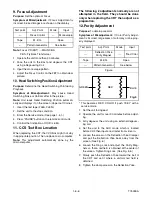
Page 26: ...crocomputer The following 2 adjustments normally are not attempted in the field They should be done only when replacing the CRT then adjust as a preparation 12 Purity Adjustment Purpose To obtain pure...

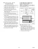
Page 27: ...at the center of the screen by rotating RB G C P Magnet See Fig 8 4 Fix the C P Magnets by tightening the Ring Lock 5 Remove the DY Wedges and slightly tilt the Deflec tion Yoke horizontally and vert...

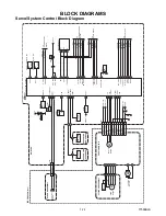
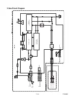
Page 28: ...KEY SWITCH KEY SWITCH SW201 SW204 SW206 SCL MEMORY SDA 6 5 REC LED 22 REC LED 23 P DOWN 84 P ON H P DOWN P ON H 31 D204 REC AL 5V LD SW 1 I 2 C OPEN 45 71 SW212 LD SW CS 7 TO POWER SUPPLY BLOCK SW205...

Page 29: ...GNAL MODE SP REC 57 QV QH 6dB AMP TO SERVO SYSTEM CONTROL BLOCK TO SERVO SYSTEM CONTROL BLOCK RF SW RF SW 59 V ENV TP202 DV SYNC DV SYNC 53 24 YCA SCLK 36 37 39 34 Q402 BUFFER 54 YCA SOUT 55 YCA CS SE...

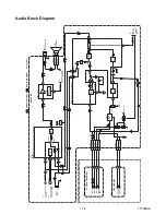
Page 30: ...801 CL802 SP MUTE TU AUDIO TO CHROMA TUNER BLOCK TP401 A OUT AUDIO HEAD AC HEAD ASSEMBLY A COM A PB REC CL402 AUDIO ERASE HEAD AE H AE H FE H 2 1 FE H FE H GND FULL ERASE HEAD CL403 3 4 6 FE HEAD UNIT...

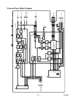
Page 31: ...VO SYSTEM CONTROL BLOCK REC VIDEO SIGNAL PB VIDEO SIGNAL Mode SP REC REC AUDIO SIGNAL WF18 WF17 WF10 WF11 TP302 AFC 56 CV IN 4 MAIN CBA 18 34 35 8 9 31 13 10 11 12 15 14 4 5 3 2 40 41 16 6 20 25 23 CH...

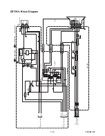
Page 32: ...F B T ANODE FOCUS SCREEN MAIN CBA CRT CBA R G B HEATER ANODE GND V501 CRT GND FOCUS SCREEN JK501 CN505 CL501A CL501B REC VIDEO SIGNAL PB VIDEO SIGNAL CN571 TO CHROMA TUNER BLOCK FOCUS VR SCREEN VR TO...

Page 33: ...12V AL 5V P ON H TO PIN31 OF IC201 5V REG 5V REG 5V REG 5V REG 8V REG IC602 Q608 Q611 Q610 Q609 Q612 5 7V REGULATOR IC301 30 27 B DEF B HOT CIRCUIT BE CAREFUL FOR CONTINUED PROTECTION AGAINST RISK OF...

Page 34: ...tely turn OFF the POWER MONITOR and switch over the Mechanical Malfunction mode with POWER OFF Shall not unload To return from this mode shall become possible only by POWER Key as in the case of the M...

Page 35: ...t keeps the function according to its mode 4 Countermeasure for CASSETTE LOADING Mal function a CASSETTE IN operating Malfunction If LD SW does not go to SB position after a lapse of 5 sec or more fro...

Page 36: ...nitors current will do Read directions below before power is added Repair method 1 Power must be off Short circuit in the secondary side check diode D613 D614 D616 D617 and D618 switching transistor Q...

Page 37: ...parts then if necessary replace with factory originals R602 is open or not Q601 Q602 D607 D608 and D611 are short or not Repair method 3 The feedback circuit which is monitored by the output of D613 1...

Page 38: ...dentified by the mark in the schematic diagram and the parts list Before replacing any of these components read the parts list in this manual carefully The use of substitute replacement parts that do...

Page 39: ...d units use only original replacement parts which are listed with their part numbers in the parts list section of the service manual 4 Wire Connectors 1 Prefix symbol CN means connector can disconnect...

Page 40: ...C2 C3 C4 D1 D2 D3 D4 E1 E2 E3 E4 F1 F2 F3 F4 Main 1 5 Schematic Diagram 1 8 3 1 8 4 T7500SCM1 MAIN 1 5 Ref No Position IC201 C 2 IC202 D 1 Q205 B 1 Q206 D 3 CL201 F 4 TP201 B 4 TP202 B 2 TEST POINTS...

Page 41: ...nal PB Video Signal PB Audio Signal Main 2 5 Schematic Diagram 1 8 5 1 8 6 T7500SCM2 MAIN 2 5 Ref No Position IC401 H 2 IC801 K 4 Q401 K 2 Q402 K 3 Q871 H 2 Q872 H 1 Q873 G 1 Q874 G 1 Q875 H 1 CL401 G...

Page 42: ...P2 P3 P4 Q1 Q2 Q3 Q4 R1 R2 R3 R4 REC Video Signal REC Audio Signal PB Video Signal PB Audio Signal Main 3 5 Schematic Diagram 1 8 7 1 8 8 T7500SCM3 MAIN 3 5 Ref No Position IC001 Q 2 IC301 M 2 Q301 N...

Page 43: ...e power supply circuit are not defective before you connect the AC plug to the AC power supply Otherwise it may cause some components in the power supply circuit to fail VOLTAGE CHART Power off mode R...

Page 44: ...Signal 1 8 11 1 8 12 T7500SCM5 Main 5 5 CRT Schematic Diagram MAIN 5 5 Ref No Position IC551 Y 3 Q571 AA 2 Q572 Z 3 Q591 Z 2 CL501B BB 3 CL502B BB 2 CN571 Z 3 CONNECTORS IC TRANSISTORS CRT Ref No Posi...

Page 45: ...iew BT5500F01011 CAUTION Fixed voltage or Auto voltage selectable power supply circuit is used in this unit If Main Fuse F601 is blown check to see that all components in the power supply circuit are...

Page 46: ...ABLE ISOLATION TRANSFORMER IS REQUIRED CAUTION FOR CONTINUED PROTECTION AGAINST RISK OF FIRE REPLACE ONLY WITH SAME TYPE 4A 125V FUSE ATTENTION UTILISER UN FUSIBLE DE RECHANGE DE M ME TYPE DE 4A 125V...

Page 47: ...WF16 Q521 Collector WF15 Q511 Collector WF14 CRT CBA Top View CRT CBA Bottom View 1 8 17 1 8 18 BT5500F01011 CRT CBA Ref No Position Q511 B 1 Q521 B 1 Q531 A 1 CL501A A 1 CL502A B 1 CN505 B 2 TRANSIST...

Page 48: ...25V 20 sec IC401 PIN 32 Upper WF6 Lower WF1 1DIV 0 2V 2DIV 5V 5msec TP402 V ENV WF5 1DIV 0 5V 20 sec TP301 V OUT WF8 1DIV 0 5V 0 5msec TP401 A OUT WF7 1DIV 0 2V 0 5msec IC001PIN 7 WF9 1DIV 0 5V 0 5ms...

Page 49: ...AUDIO ERASE HEAD M LOADING MOTOR CYLINDER ASSEMBLY CL201 CAPSTAN MOTOR M DRUM MOTOR PG SENSOR CL402 1 FE H GND 2 FE H 1 P ON 12V 2 P ON 5V 2 3 C FG 4 C F R 5 C CONT 6 FG GND 7 LD CONT 8 D CONT 9 D PFG...

Page 50: ...LD REV 0 2S 0 5S PIN NO CL EJ SS SS AU AU TL LD SW CL SS LD CONT C DRIVE Z ON ON C F R DRUM ROTATION P ON A MUTE H D REC H D PB H PAUSE ON PAUSE PAUSE ON PAUSE OFF PAUSE OFF AU AL AU SF SM EJ AU RS S...

Page 51: ...P A LD REV FF LD REV LD REV LD FWD LD FWD LD FWD LD FWD LD FWD LD FWD LD FWD REC PAUSE REC REC REW LD REV LD REV LD REV LD REV LD REV LD REV LD REV PAUSE REC or PAUSE STOP EJECT STOP EJECT STOP EJECT...

Page 52: ...26 FM TV SW FM TV SW Signal 27 NU Not Used 28 NU Not Used 29 NU Not Used 30 NU Not Used 31 OUT P ON H Power On Signal at High 32 NU Not Used 33 IN REC SAFETY Record Protection Tab Detection 34 IN RES...

Page 53: ...L Take Up Reel Rotation Signal 81 NU Not Used 82 OUT LD CONT Loading Motor Control Signal 83 NU Not Used 84 IN P DOWN Power Voltage Down Detector Signal 85 NU Not Used 86 GND GND 87 IN C FG Capstan Mo...

Page 54: ...27Y TPE2 2SC2482 TPE6 2SC2785 F H J BN1F4M T KTA1267 GR KTA1271 Y KTC3199 GR 2SC1815 GR TPE2 2SC2120 O Y TPE2 2SC3331 T U KRA103M KTC3203 Y LA78040A 2SC5885000RF TT2140LS YB11 MID 32A22F PT204 6B 12 K...

Page 55: ...1 2 L1 L1 L1 L1 B5 A3 A2 A1 1 A1 4 A1 2 A1X A1 3 A1 6 A1 5 B2 B2 B2 B2 B1 B4 B4 A4 L4 L4 B11 CL802 SP801 L2 TL1 TL1 TL1 TL1 TB26 TB9 1B1 TL2 TL5 TL2 TL2 TL4 TB3 TB1 TB10 TB21 TB7 CRT CBA MAIN CBA W601...

Page 56: ...1 14 3 T7500PEX Packing X1 S1 S4 S3 S3 S2 TAPE TAPE X4 X3 X2 X7 S6 S14 FRONT...

Page 57: ...TJ T7400UA TB24 WIRE HOLDER T5400UA 0EM407678 TL1 SCREW P TIGHT 3X12 WASHER HEAD GCMP3120 TL3 SCREW S TIGHT 3X4 BIND HEAD GBMS3040 TL4 SCREW B TIGHT M3X8 BIND HEAD GBMB3080 TL5 SCREW P TIGHT M3X8 BIND...

Page 58: ...0BV001 CRT TYPE F L551 DEFLECTION YOKE 330P510A37 LLBY00ZTHA01 V501 CRT A48LGS30X TCRT190THA01 V501 1 C P MAGNET JH225 014 or XM04000BV009 CPM E 225 F01 XM04000ETC01 V501 2 WEDGE FT 00110W XV10000T400...

Page 59: ...28 C216 CHIP CERAMIC CAP F Z 0 01 F 50V CHD1JZB0F103 C217 CHIP CERAMIC CAP SL D 10pF 50V CHD1JDBSL100 C218 CHIP CERAMIC CAP CH J 15pF 50V CHD1JJBCH150 C219 CHIP CERAMIC CAP B K 0 01 F 50V CHD1JKB0B103...

Page 60: ...1000 F 25V M CE1EMZPTL102 C558 CERAMIC CAP AX B K 0 01 F 50V CA1J103TU011 C559 ELECTROLYTIC CAP 330 F 35V M or CE1GMASDL331 ELECTROLYTIC CAP 330 F 35V M CE1GMASTL331 C560 FILM CAP P 0 01 F 100V J CMA...

Page 61: ...NNECTOR BASE 00 8283 0212 00 000 or J383C02UG002 STRAIGHT PIN HEADER 2P 173981 2 1770258 DIODES D031 SWITCHING DIODE 1SS133 T 77 or QDTZ001SS133 SWITCHING DIODE 1N4148 NDTZ001N4148 D203 LED SIR 563ST3...

Page 62: ...IODE 1N4148 NDTZ001N4148 D638 SWITCHING DIODE 1SS133 T 77 or QDTZ001SS133 SWITCHING DIODE 1N4148 NDTZ001N4148 D639 SCHOTTKY BARRIER DIODE 11EQS04 or QD4Z011EQS04 SCHOTTKY BARRIER DIODE ERA81 004 QDPZE...

Page 63: ...STOR BN1F4M T QQSZ00BN1F4M Ref No Description Part No RESISTORS R002 CHIP RES 1608 1 10W J 100 RRXAJB5Z0101 R003 CHIP RES 1608 1 10W J 100 RRXAJB5Z0101 R032 CHIP RES 1608 1 10W J 100 RRXAJB5Z0101 R033...

Page 64: ...J 3 9M RRXAJB5Z0395 R424 CHIP RES 1608 1 10W J 100k RRXAJB5Z0104 R425 CHIP RES 1608 1 10W J 82k RRXAJB5Z0823 Ref No Description Part No R426 CHIP RES 1608 1 10W J 2 2k RRXAJB5Z0222 R427 CARBON RES 1...

Page 65: ...AJB5Z0223 R852 CHIP RES 1608 1 10W J 3 3k RRXAJB5Z0332 R853 CHIP RES 1608 1 10W J 2 2M RRXAJB5Z0225 Ref No Description Part No R856 CARBON RES 1 4W J 22k RCX4JATZ0223 R857 CHIP RES 1608 1 10W J 3 9k R...

Page 66: ...U 10 6MHz or FXD106LLN001 X TAL AT49 10 6 FXD106LDS002 X301 X TAL 3 579545 MHz or FXD355LLN003 X TAL 3 579545MHz 30PPM FXD355LCHE01 X401 X TAL 3 579545MHz 20PPM or FXC355LLN003 X TAL 3 579545MHz 20PP...

Page 67: ...on Part No SENSOR CBA Consists of the following 0ESA06170 TRANSISTORS Q201 PHOTO TRANSISTOR MID 32A22F or NPWZ1D32A22F PHOTO TRANSISTOR PT204 6B 12 NPWZT2046B12 Q202 PHOTO TRANSISTOR MID 32A22F or NPW...

Page 68: ...WF319E 6319CE T7500UA T7502UC 2004 02 26...

Reviews: