background image

1-4-4

SFTY_5

Instructions for Handling 
Semiconductors

Electrostatic breakdown of the semiconductors may
occur due to a potential difference caused by electro-
static charge during unpacking or repair work.

Ground for Human Body

Be sure to wear a grounding band (1M

) that is prop-

erly grounded to remove any static electricity that may
be charged on the body.

Ground for Work Bench

Be sure to place a conductive sheet or copper plate
with proper grounding (1M

) on the work bench or

other surface, where the semiconductors are to be
placed. Because the static electricity charge on the
clothing will not escape through the body grounding
band, be careful to avoid contacting semiconductors to
clothing.

CBA

<Incorrect>

CBA

Grounding Band

Conductive Sheet or
Copper Plate

1M

1M

<Correct>
Summary of Contents for 6719DC

Page 1: ...ion for Servicing I Adjustment Procedures I Schematic Diagrams I CBA s Sec 2 Deck Mechanism Section I Standard Maintenance I Alignment for Mechanism I Disassembly Assembly of Mechanism Sec 3 Exploded...

Page 2: ...e equipment It also is important to understand that these CAUTIONS and NOTICES ARE NOT EXHAUSTIVE Funai could not possibly know evaluate and advice the service trade of all conceivable ways in which s...

Page 3: ...nd Functions 1 6 1 Cabinet Disassembly Instructions 1 7 1 Electrical Adjustment Instructions 1 8 1 FIRMWARE Renewal Mode 1 9 1 Block Diagrams 1 10 1 Schematic Diagrams CBA s and Test Points 1 11 1 Wav...

Page 4: ...m 2 5 Side m m 1 5 2 Tint Control Range deg 30 3 Contrast Control Range dB 6 2 4 Brightness 100 White Full Field Contrast Max ft L 35 24 5 Color Temperature K 9200 Description Condition Unit Nominal L...

Page 5: ...Limit 1 Horizontal Resolution R P SP Line 230 200 2 Jitter Low R P SP S 0 1 0 2 3 S N Chroma AM SP R P SP dB 38 33 PM SP R P SP dB 38 33 4 Wow Flutter JIS UNWTD R P SP 0 25 0 5 Description Condition...

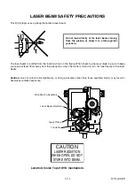
Page 6: ...ion shown in the figure When checking the laser diode be sure to keep your eyes at least 30cm away from the pickup lens when the diode is turned on Do not look directly at the laser beam Caution Use o...

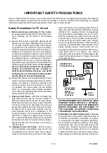
Page 7: ...ongs tied together and touch the other ohmme ter lead in turn to each tuner antenna input ex posed terminal screw and if applicable to the coaxial connector If the measured resistance is less than 1 0...

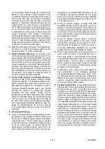
Page 8: ...ed to the ground side of the AC power source To confirm that the AC power plug is inserted correctly with an AC volt meter measure between the chassis and a known earth ground If a voltage reading in...

Page 9: ...ot contact sharp edged or pointed parts H When a power cord has been replaced check that 5 6 kg of force in any direction will not loosen it I Also check areas surrounding repaired locations J Be care...

Page 10: ...er cord plug prongs and externally exposed accessible parts RF terminals antenna terminals video and audio input and output terminals microphone jacks earphone jacks etc Measuring Method Power ON Inse...

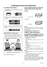
Page 11: ...s The Following Procedures are Recom mended for the Replacement of the Leadless Components Used in this Unit 1 Preparation for replacement a Soldering Iron Use a pencil type soldering iron less than 3...

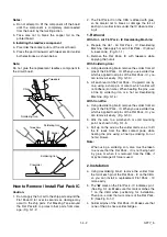
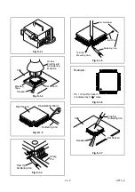
Page 12: ...ins of the Flat Pack IC you can remove it easily Fig S 1 3 b Lift each lead of the Flat Pack IC upward one by one using a sharp pin or wire to which solder will not adhere iron wire When heating the p...

Page 13: ...Tape Fig S 1 3 Flat Pack IC Desoldering Braid Soldering Iron Fig S 1 4 Fine Tip Soldering Iron Sharp Pin Fig S 1 5 To Solid Mounting Point Soldering Iron Iron Wire or Hot Air Blower Fig S 1 6 Example...

Page 14: ...ded to remove any static electricity that may be charged on the body Ground for Work Bench Be sure to place a conductive sheet or copper plate with proper grounding 1M on the work bench or other surfa...

Page 15: ...ism assembly is removed from the Main CBA due to servicing this switch can not be oper ated automatically Preparing 2 1 To eject the tape press the STOP EJECT button on the unit or Remote Control 2 Wh...

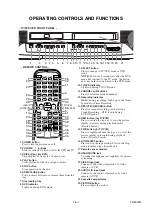
Page 16: ...tput jack of a video camera or VCR 20 AUDIO L R input jacks Connect to the audio output jacks of a video camera or VCR 21 Cassette compartment 22 PICTURE button Press to adjust the picture REMOTE CONT...

Page 17: ...o select a desired subtitle language 35 REPEAT button Repeats playback of the current disc title chapter or track 36 ANGLE button DVD mode Press to change the camera angle to see the sequence being pl...

Page 18: ...S Screw P Spring L Locking Tab CN Connec tor Unhook Unlock Release Unplug or Desolder 2 S 2 two Screw S 2 5 Refer to the following Reference Notes in the Table ID LOC No PART REMOVAL Fig No REMOVE UN...

Page 19: ...used by electrostatic charge accumulated on cloth human body etc during unpacking or repair work To avoid damage of pickup follow next procedures 2 1 Slide the pickup unit as shown in Fig 5 2 2 Short...

Page 20: ...1 7 3 TD500DC Fig 1 ANT 1 S 1 S 1 S 1 S 1 S 3 S 2 1 REAR CABINET Fig 2 S 1 S 1 S 2 S 3 S 1 S 1 S 1 S 1 1 REAR CABINET...

Page 21: ...3 S 5 S 5 5 Shield Box 3 Tray Chassis 2 H V CBA wih Holder H V CBA 6 DVD Mechanism 11 Deck Assembly 12 Main CBA 8 Filter CBA 9 Bottom Plate 10 Power Supply AV CBA S 6 S 8 S 9 S 9 S 8 S 8 S 10 S 10 S...

Page 22: ...RT Anode Cap CRT CBA Fig 4 Fig 5 CN101 DVD Mechanism 7 DVD Main CBA Unit CN401 S 7 S 7 S 7 View for B Pickup Unit C B Short the three short lands by soldering View for C Slide View for A OR Short the...

Page 23: ...CN403 CN402 CN404 CN401 FILTER CBA TO POWER SUPPLY AV CBA SPEAKER CN2401 CN2402 CN2601 CN2801 CN2802 CN2803 CN2804 CN2602 ANODE CRT GND TUNER MAIN CBA CN1802 CN1302 CN1301 CN1805 CN1804 CN1803 CL1403...

Page 24: ...rvice Mode 1 Use the service remote control unit 2 Turn the power on Use main power on the TV unit 3 To enter the TV mode press CH UP or CH DOWN button on the TV unit 4 Press DISC MENU button on the s...

Page 25: ...t Level 60dB V 3 Press CH o p buttons so that the voltage of TP1001 AGC becomes 2 8V 0 3V DC 4 Turn the power off and on again 4 1 H Adjustment Purpose To get correct horizontal position and size of s...

Page 26: ...V S Mode Press 9 button then display will change to V P and V S 2 Input monoscope pattern 3 Press CH o p buttons on the remote control unit so that the monoscope pattern is 90 5 of display size and t...

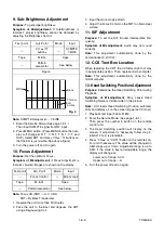
Page 27: ...ontal line appears on the CRT 4 Press the VOL p button Press VOL p then display will change CUT OFF DRIVE VCO adjustment 7Fh adjustment 5 Choose CUT OFF DRIVE Mode then press 1 but ton This adjustment...

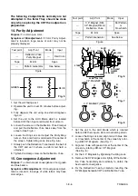
Page 28: ...e chrominance IC IC1301 12 CCS Text Box Location When replacing the CRT the CCS Box might not stay in appropriate position Then replace micro computer Note This adjustment automatically done by the mi...

Page 29: ...convergence of red green and blue beams Symptom of Misadjustment If Convergence Adjust ment is incorrect the edge of white letters may have color edges 1 Set the unit to the AUX Mode which is located...

Page 30: ...The appearance shown in 2 of Fig B is described as follows 7 After programming is finished the tray opens auto matically Fig C appears on the screen At this time no buttons are available 8 For tray o...

Page 31: ...1 10 2 TD500BLS SCL MEMORY SDA 6 5 P DOWN L 84 P ON H P DOWN L P ON H 31 LD SW 1 I 2 C OPEN EXT H 45 71 AL 5V SW1212 LD SW CS 7 FROM TO POWER SUPPLY BLOCK DIAGRAM SDA SCL FROM TO CHROMA TUNER BLOCK D...

Page 32: ...RAM RF SW TP1401 WF1 TP1403 ENV BUFFER DV SYNC TAPE SPEED TAPE SPEED ROTA DV SYNC ROTA 14 36 16 71 39 59 73 SPL PLAY REC EE PB RENTAL SPL PLAY REC EE PB RENTAL 42 EXT H 74 45 47 49 44 Q1402 BUFFER WF6...

Page 33: ...C H EXT H A MUTE H EXT H FROM SERVO SYSTEM CONTROL BLOCK DIAGRAM 4 78 11 WF7 WF8 3 1 EQ AMP 100 SP LP ON 2 IC2202 OUTPUT SELECT IC2801 AUDIO AMP DC VOL IC2203 OP AMP SP R 1 SP GND 2 SPEAKER R CH JK180...

Page 34: ...N A OUT FROM CHROM TUNER BLOCK DIAGRAM AGC AGC DET 49 A OUT L A OUT R N A IN Hi Fi SW A MUTE H NORMAL H 51 ST SAP IN FROM TO AUDIO BLOCK DIAGRAM Hi Fi DATA Hi Fi CLK Hi Fi CS P ON 9V FROM SERVO SYSTEM...

Page 35: ...O CONNECTION CN1303 is used for adjustment at factory INT MONITOR 1 2 SDA 4 SCL 5 I 2 C OPEN I 2 C OPEN 2 MAIN CBA POWER SUPPLY AV CBA 34 6 5 19 20 43 24 21 22 23 27 63 64 59 26 16 33 15 14 10 11 18 3...

Page 36: ...CN501 CL501B CL501A REC VIDEO SIGNAL PB VIDEO SIGNAL DVD VIDEO SIGNAL CN571 P ON 180V 3 3 FROM TO CHROMA TUNER BLOCK DIAGRAM CN1302 11 S F HV FOCUS VR SCREEN VR 1 10 12 1 10 11 FROM POWER SUPPLY BLOCK...

Page 37: ...2601 IC1602 P DOWN L TO PIN84 OF IC1201 Q2604 VR2601 B ADJ Q2602 FEED BACK 5V REG 12 13 1 B 2 B 4 DEF B 4V REG IC2615 1 2 5 1 8V REG IC2617 1 2 4 SW CTL IC2616 Q1608 SW 5V Q1611 SW 5V Q1613 SW 5V Q160...

Page 38: ...LK 204 125 REMOTE CN501 CN403 DVD MAIN CBA UNIT FILTER CBA FG CBA RELAY CBA BLOCK DIAGRAMS DVD Section TREV TIN TOUT TFWD MUTE PS CD DVD CFE CAS STANDBY ADDRESS BUS DATA BUS CD DVD CFE CAS STANDBY 71...

Page 39: ...102 AMP FOCUS MOTOR DRIVE TRACKING MOTOR DRIVE LOADING MOTOR DRIVE SPINDLE MOTOR DRIVE POWER SAVE SLIDE MOTOR DRIVE LOADING MOTOR SPINDLE MOTOR SLIDE MOTOR M 5 21 2 1 23 26 25 27 22 24 4 67 115 114 11...

Page 40: ...LICER PLL VCO CPU INTERFACE VIDEO AUDIO INTERFACE DVD DEMODULATOR MEMORY MANAGER 172 168 166 164 160 158 151 149 82 TO DVD VIDEO BLOCK DIAGRAM BCA DATA VIDEO AUDIO SIGNAL DVD MAIN CBA UNIT FROM TO DVD...

Page 41: ...17 DATA VIDEO AUDIO SIGNAL RAS CAS LDQM UDQM WE RAS CAS 58 63 66 73 74 19 CS CS INTERNAL PERIPHERALS PORTS PROGRAMMABLE CPU INTERFACE CENTRAL COMMAND PORT FRONT END LINK INTERFACE ST20 ARBITER MEMORY...

Page 42: ...RIAL PORT SERIAL CONTROL 4X 8X OVERSAMPLING DIGITAL FILTER FUNCTION CONTROLLER ENPHANCED MULTI LEVEL DELTA SIGMA MODULATOR DAC LPF AMP L CH R CH LPF AMP DAC ZERO DETECT SYSTEM CLOCK PCM BCK SPDIF PCM...

Page 43: ...identified by the mark in the schematic diagram and the parts list Before replacing any of these components read the parts list in this manual carefully The use of substitute replacement parts that d...

Page 44: ...ts use only original replacement parts which are listed with their part numbers in the parts list section of the service manual 4 Wire Connectors 1 Prefix symbol CN means connector can disconnect and...

Page 45: ...l 1 11 3 1 11 4 1 11 5 TD500SCM1 Main 1 4 Schematic Diagram TV VCR Section MAIN 1 4 Ref No Position IC1201 D 4 IC1202 F 5 IC1602 B 2 Q1205 D 2 Q1206 E 5 Q1207 B 3 Q1210 B 3 Q1211 B 3 Q1608 B 1 Q1609 B...

Page 46: ...REC Video Signal 1 11 6 1 11 7 1 11 8 TD500SCM2 Main 2 4 Schematic Diagram TV VCR Section MAIN 2 4 Ref No Position IC1401 I 2 Q1401 K 2 Q1402 L 4 Q1403 L 4 Q1491 L 2 Q1871 I 2 Q1872 I 2 Q1873 I 1 Q187...

Page 47: ...T4 T5 U1 U2 U3 U4 U5 T2 PB Video DVD Video Signal REC Video Signal 1 11 9 1 11 10 1 11 11 TD500SCM3 Main 3 4 Schematic Diagram TV VCR Section MAIN 3 4 Ref No Position IC1301 R 2 Q1301 R 5 Q1302 Q 4 C...

Page 48: ...PB Video DVD Video Signal PB Audio Signal PB Video Signal DVD Video Signal REC Audio Signal REC Video Signal 1 11 12 1 11 13 1 11 14 TD500SCM4 Main 4 4 Schematic Diagram TV VCR Section MAIN 4 4 Ref No...

Page 49: ...53 C 2 J563 B 2 TEST POINTS IC CONNECTORS H V TRANSISTORS CORRECTION SHEET TV DVD VCR COMBINATION Models 6719DC SSC719C EWC19T2 H V Schematic Diagram TV VCR Section on page 1 11 15 16 of SCHEMATIC DIA...

Page 50: ...1 C2 PB Video DVD Video Signal REC Video Signal CRT Schematic Diagram TV VCR Section TD500SCCRT 1 11 17 1 11 18 CRT Ref No Position Q501 B 2 Q502 B 2 Q503 B 1 CL501B A 2 CL504B A 2 CN501 C 1 TRANSISTO...

Page 51: ...the AC plug to the AC power supply Otherwise it may cause some components in the power supply circuit to fail CAUTION FOR CONTINUED PROTECTION AGAINST FIRE HAZARD REPLACE ONLY WITH THE SAME TYPE FUSE...

Page 52: ...G2 G3 G4 G5 Tracking Servo Signal Focus Servo Signal DATA Video Audio Signal 1 11 22 1 11 23 1 11 24 TD500SCD1 DVD Main 1 4 Schematic Diagram DVD Section MAIN 1 4 Ref No Position IC101 C 4 IC102 F 5 I...

Page 53: ...N2 N3 N4 N5 Tracking Servo Signal Focus Servo Signal Slide Servo Signal Spindle Servo Signal DATA Video Audio Signal DVD Main 2 4 Schematic Diagram DVD Section 1 11 25 1 11 26 1 11 27 TD500SCD2 MAIN 2...

Page 54: ...U2 U3 U4 O5 P5 Q5 R5 S5 T5 U5 DATA Video Audio Signal DATA Video Signal DATA Audio Signal DVD Video Signal DVD Main 3 4 Schematic Diagram DVD Section 1 11 28 1 11 29 1 11 30 TD500SCD3 MAIN 3 4 Ref No...

Page 55: ...V1 V2 V3 W1 W2 W3 X1 X2 X3 Y1 Y2 Y3 Z1 Z2 Z3 AA3 AA2 AA1 DATA Audio Signal DVD Video SIGNAL DVD Audio Signal DVD Main 4 4 Schematic Diagram DVD Section TD500SCD4 1 11 31 1 11 32...

Page 56: ...2 C3 C4 DATA Audio Signal DVD Video SIGNAL DVD Audio Signal Filter Schematic Diagram DVD Section TD500SCF 1 11 33 1 11 34 Ref No Position CN401 C 4 CN402 C 2 CN403 A 4 CN404 A 2 TP401 C 1 TP402 B 1 FI...

Page 57: ...CBA Top View TV VCR Section 1 11 35 1 11 36 BT5200F01023 A Ref No Position Ref No Position IC551 B 2 CL503A C 2 CN571 A 1 Q571 B 1 Q572 C 1 J551 A 2 Q591 C 1 J552 B 2 J553 B 2 CL501A B 2 J563 B 2 CL50...

Page 58: ...PIN 5 OF CN571 WF12 Q571 Collector WF11 1 11 37 1 11 38 BT5200F01023 A H V CBA Bottom View TV VCR Section...

Page 59: ...1 E 5 IC1401 C 3 IC1601 F 2 IC1602 F 1 IC1751 D 2 Q1205 B 2 Q1206 B 3 Q1207 A 1 Q1210 A 1 Q1211 A 1 Q1301 F 4 Q1302 F 4 Q1401 B 3 Q1402 C 3 Q1403 B 2 Q1491 C 4 Q1601 F 2 Q1602 F 2 Q1603 F 2 Q1608 F 2...

Page 60: ...1401 WF2 PIN 61 OF IC1401 WF4 PIN 42 OF IC1401 WF17 PIN 59 OF IC1201 WF16 PIN 58 OF IC1201 WF10 WF8 PIN 11 OF IC1301 PIN 20 OF IC1301 WF9 1 11 42 1 11 43 1 11 44 BTD500F01012 Main CBA Bottom View TV V...

Page 61: ...HAZARD REPLACE ONLY WITH THE SAME TYPE FUSE ATTENTION POUR UNE PROTECTION CONTINUE LES RISQES D INCELE N UTILISER QUE DES FUSIBLE DE MEMO TYPE RISK OF FIRE REPLACE FUSE AS MARKED This symbol means fa...

Page 62: ...UIT AN ISOLATION TRANSFORMER MUST BE USED ALSO IN ORDER TO HAVE THE ABILITY TO INCREASE THE INPUT SLOWLY WHEN TROUBLESHOOTING THIS TYPE POWER SUPPLY CIRCUIT A VARIABLE ISOLATION TRANSFORMER IS REQUIRE...

Page 63: ...or WF14 Q503 Collector WF15 CRT CBA Top View TV VCR Section 1 11 51 1 11 52 BT5200F01023 B CRT CBA Bottom View TV VCR Section CRT CBA Ref No Position Q501 B 1 Q502 B 1 Q503 A 2 CL501B B 1 CL504B A 1 C...

Page 64: ...tion B CBA Top View TV VCR Section Junction B CBA Bottom View TV VCR Section BT5200F01023 C 1 11 53 1 11 54 Filter CBA Top View DVD Section Filter CBA Bottom View DVD Section BTD500F01022 B Ref No Pos...

Page 65: ...1301 PIN 11 WF9 MAIN 3 4 SCHEMATIC DIAGRAM IC1301 PIN 20 WF12 H V SCHEMATIC DIAGRAM CN571 PIN 5 WF14 CRT SCHEMATIC DIAGRAM Q502 COLLECTOR WF15 CRT SCHEMATIC DIAGRAM Q503 COLLECTOR WF11 H V SCHEMATIC D...

Page 66: ...F18 WF20 WAVEFORMS DVD Section WF23 SPDIF Pin 11 of CN2402 1V 0 2usec WF18 Pin 14 of CN2402 WF20 Pin 18 of CN2402 WF21 DVD AUDIO L Pin 5 of CN2402 1V 0 5msec WF22 DVD AUDIO R Pin 7 of CN2402 1V 0 5mse...

Page 67: ...C F R 2 P ON 5V 3 3 D L 12V 4 FG GND 5 C FG 6 C CONT 7 M GND 8 D FG 9 LD CONT 10 D CONT 11 D PG 12 CL1201 CL1401 GND 1 GND 2 P ON 9V 1 3 AL 33V 4 SAFETY 5 P ON 9V 2 6 NU 7 AL 9V 8 GND 9 DVD Y 13 DVD C...

Page 68: ...8 GND 8 7 GND 13 2 DVD VIDEO 12 3 GND 11 4 DVD C 10 5 GND 9 6 CN701 CN404 EV 2 5V 24 3 2 25 1 26 NU REMOTE CN3001 SW CBA M M SPINDLE MOTOR SLIDE MOTOR RELAY CBA 19 20 21 GND CD PD CD LD CD DVD 1 2 3...

Page 69: ...SF 1 51V 1 98V 1 80V AU 3 20V 3 75V 3 40V AL 0 26V 0 65V 0 44V SS 4 51V 5 00V 5 00V GC 2 61V 3 19V 2 97V RS Note Note EJ RS Loading FWD LM FWD H LM REV L RS EJ Loading REV LM FWD L LM REV H Stop A Loa...

Page 70: ...Signal C DRIVE PB CTL 66 C F R 16 H A SW 15 ROTA AT H Z H L L ST BL STILL FRAME ADVANCE STILL The first rise of RF SW after a rise in F AD signal Stop detection T2 Slow Tracking Value Acceleration De...

Page 71: ...D Internal Signal C DRIVE PB CTL 66 C F R 16 H A SW 15 ROTA STILL STILL AT ST BL Stop detection T2 Acceleration Detection T1 Slow Tracking Value Reversal Limit Value FRAME ADVANCE The first rise of RF...

Page 72: ...REV LD REV LD FWD LD FWD LD REV LD REV LD REV 0 5S PIN NO CL EJ SB TL SB GC FB GC SS AL SS AU AU TL 1 LD SW CL GC 82 LM FWD M REV C DRIVE Z ON ON 66 C F R DRUM ROTATION 31 P ON POWER OFF STOP PLAY RS...

Page 73: ...REV LD REV LD REV FF PIN NO SF FB TL AL GC FB GC SS AL SS AU AU TL 1 LD SW CL GC 82 LM FWD M REV C DRIVE Z ON ON 66 C F R DRUM ROTATION 31 P ON STOP FF STOP REW STOP REC REC REC PAUSE STOP 65 A MUTE H...

Page 74: ...LSW2 LSW1 LM LM I o TL123 SP TP122 Tv TL122 0V 5V 0V Tray close Tray open Tray close Play Play Tray open Play 0V Eject key on 6V 2V 5V 0V Disc Rotation Eject key on 2V 2 0s 0V 6V 4 4s 1 2s 700ms 1 7s...

Page 75: ...L H Audio Mode Input Signal 23 OUT ACL CONT ACL Control Signal 24 NU Not Used 25 OUT REM OUT DVD REMOTE SIGNAL 26 OUT TV VCR LED TV VCR Mode LED Control Signal 27 IN OUT REC EE PB YCA IC Mode Output 2...

Page 76: ...Motor Control Signal 77 OUT D CONT Drum Motor Control Signal 78 NU Not Used 79 NU Not Used 80 IN T REEL Take Up Reel Rotation Signal 81 NU Not Used 82 OUT LD CONT Loading Motor Control Signal 83 NU N...

Page 77: ...F PC817X6 A C S D G 2SK2662 2SK3407 E C B 2SD400 F LA78040A AN5522 1 7 48 33 49 M612106FP R61 M612106FP R62 32 17 16 1 64 M37760MCH4D8GP LA71091M 80 51 81 100 1 30 50 31 5 4 8 1 BR24C02F W BR24C02F A...

Page 78: ...vice Fixtures and Tools 2 2 1 Mechanical Alignment Procedures 2 3 1 Disassembly Assembly Procedures of Deck Mechanism 2 4 1 Alignment Procedures of Mechanism 2 4 9 Sec 2 Deck Mechanism Section I Stand...

Page 79: ...ove refer to Deck Exploded Views B73 Recording Model only H Hours Check I Change Deck Periodic Service Schedule Ref No Part Name 1 000 H 2 000 H 3 000 H 4 000 H B2 Cylinder Assembly I I B3 Loading Mot...

Page 80: ...hard material but since it is very thin avoid cleaning it vertically 2 Wait for the cleaned part to dry thoroughly before operating the unit 3 Do not reuse a stained head cleaning stick or a stained c...

Page 81: ...Alignment Tape FL8N 2Head only FL8NW 4Head only Azimuth and X Value Adjustment of Audio Control Head Adjustment of Envelope Waveform J 2 Guide Roller Adj Screwdriver Available Locally Guide Roller J...

Page 82: ...that the Moving guide preparations are in the Eject Position 4 Turn the LDG Belt in the appropriate direction shown in Fig M1 until the Moving guide prepara tions come to the Eject Position Stop turni...

Page 83: ...the X value and envelope Not good Do the final tape traveling test to see that the tape runs normally in play mode with out creasing or slacking Completion Not good OK OK OK Not good Not good OK Flowc...

Page 84: ...of the Audio Control Erase Head Symptom of Misalignment If the Horizontal Position of the Audio Control Erase Head is not properly aligned maximum envelope can not be obtained at the Neutral position...

Page 85: ...eight of Guide Roller 2 Refer to Fig M3 so that the waveform looks like the one shown in Fig M9 4 If the envelope is as shown in Fig M8 adjust the height of Guide Roller 3 Refer to Fig M3 so that the...

Page 86: ...lder 3 S 5 8 8 Loading Motor Assembly T DM1 DM7 Desolder LDG Belt 2 S 6 9 9 AC Head Assembly T DM1 DM7 S 7 10 2 Tape Guide Assembly T DM1 DM8 P 2 11 10 Door Opener B T DM1 DM8 L 1 L 2 12 11 Pinch Arm...

Page 87: ...ion for Installation Refer to Deck Exploded Views for lubrication 33 2 25 M Brake T Assembly T DM1 DM16 P 6 34 2 25 M Brake S Assembly T DM1 DM16 P 7 35 34 Tension Lever Sub Assembly T DM1 DM16 36 35...

Page 88: ...2 4 3 TD601DA 14 13 11 10 12 7 46 8 29 40 38 37 39 42 41 43 9 33 15 35 36 34 Fig DM1 Top View Fig DM2 Bottom View 31 19 32 24 25 27 26 23 28 21 30 20 22...

Page 89: ...shing the locking tab as shown in the right slide and pull up the right side on 2 to release Pin A and Pin B from the slots A Then remove Pin C and Pin D on 2 from the slots B as shown 1 2 A Fig DM4 3...

Page 90: ...of 12 are in the grooves of 28 as shown 11 13 12 A 10 L 1 P 3 Adj Screw P 2 L 2 View for A Fig DM8 14 15 S 9 S 8 Fig DM9 17 16 18 S 10 L 3 After removing the Screw S 10 while pressing the Locking Tab...

Page 91: ...2 4 6 TD601DA 19 S 11 Cap Belt Fig DM11 20 C 1 A 21 Portions A Portions A View for A Portions A on 21 must be set in the slot on 20 as shown Fig DM12...

Page 92: ...Pin of 30 Position of Mode Lever when installed Pin of 34 Fig DM14 23 P 4 C 3 P 4 28 28 23 When installing 23 install the spring P 4 to 28 as shown in the left figure and then install 23 while pressin...

Page 93: ...2 4 8 TD601DA 32 30 29 L 5 P 5 31 Refer to the Alignment Section Page 2 4 9 Fig DM15 L 6 P 7 P 6 C 6 34 40 37 35 39 33 36 turn turn turn 38 C 7 Fig DM16 41 42 43 L 7 Fig DM17 45 44 Slide Fig DM18 P 8...

Page 94: ...the mechanical or electrical parts Alignment points in Eject Position Alignment 1 Loading Arm S and T Assembly Install Loading Arm S and T Assembly so that their triangle marks point to each other as...

Page 95: ...y Install the Rack Assembly so that the first tooth on the gear of the Rack Assembly meets the first groove on the Cam Gear A as shown in Fig AL4 Cam Gear A First tooth First groove on the Cam Gear A...

Page 96: ...EWC19T2 TABLE OF CONTENTS Cabinet Exploded Views 3 1 1 Packing Exploded Views 3 1 3 Deck Mechanism Exploded Views 3 1 4 Mechanical Parts List 3 2 1 Electrical Parts List 3 3 1 Deck Parts List 3 4 1 S...

Page 97: ...A4 L4 L4 B6 L4 L4 B6 DL2 DL2 DB2 DB4 DL1 DL1 DB1 A1 4 A1 6 A1 5 L1 L1 L1 L3 A3 A2 L2 L1 L1 L1 B5 B5 A1X V501 1 L551 Details for L551 and surrounding parts SHINWHA TAPE SGT 730 WHITE SHINWHA TAPE SGT...

Page 98: ...3 1 3 TD500PEX Packing S7 PACKING TAPE S6 X5 TAPE S4 X1 X2 X4 X3 S3 S1 S2...

Page 99: ...ription Part No SLIDUS OIL 150 0VZZ00226 B2 B35 B553 B410 B411 B494 B567 L1053 B74 B10 L1191 B73 B9 B12 B492 B11 B571 B37 B126 L1466 B501 B8 B121 B426 B560 L1450 L1051 L1467 Floil G 374G 0VZZ00109 Blu...

Page 100: ...8 B551 B133 B568 B569 B513 B502 B570 B491 B565 B417 L1151 B525 B522 B31 L1406 B148 B521 B520 B416 B518 B564 B585 B487 B573 B574 B499 B27 B587 B508 B414 B505 B572 B558 B557 B3 Mark Description Part No...

Page 101: ...L1341 L1341 L1321 B347 L1321 Note There are two different but interchangeable types of CLEANER LEVER B359 in this model and have different combination with B361 Please see Table 1 for details and com...

Page 102: ...G601 DEGAUSSING COIL F 039 or LLBH00ZTM039 DEGAUSSING COIL AVDG106 LLBH00ZWR038 L1 SCREW P TIGHT 4X18 BIND HEAD GBMP4180 L2 SCREW TAPPING M4X14 DBU14140 L3 SCREW P TIGHT 3X10 BIND HEAD GBKP3100 L4 SCR...

Page 103: ...chart for parts order CRT Warning Label Location V501 2 WEDGE FT 00110W XV10000T4001 V501 3 RUBBER MAGNET 20X10X1 2 XM05000BV001 CRT TYPE B L551 DEFLECTION YOKE CDY M2023F LLBY00ZQS005 V501 CRT A48LRH...

Page 104: ...C CAP AX CH J 100pF 50V CA1J101TU008 C1232 CERAMIC CAP AX CH J 100pF 50V CA1J101TU008 C1233 CERAMIC CAP AX Y M 0 01 F 16V CCA1CMT0Y103 C1235 CERAMIC CAP AX Y M 0 01 F 16V CCA1CMT0Y103 C1238 CERAMIC CA...

Page 105: ...E1JMASSL1R0 C1426 ELECTROLYTIC CAP 22 F 16V M H7 CE1CMASSL220 Ref No Description Part No C1427 CERAMIC CAP AX Y M 0 01 F 16V CCA1CMT0Y103 C1428 CERAMIC CAP AX Y M 0 01 F 16V CCA1CMT0Y103 C1429 ELECTRO...

Page 106: ...C1787 ELECTROLYTIC CAP 22 F 50V M or CE1JMASDL220 ELECTROLYTIC CAP 22 F 50V M CE1JMASTL220 C1788 ELECTROLYTIC CAP 4 7 F 50V M or CE1JMASDL4R7 Ref No Description Part No ELECTROLYTIC CAP 4 7 F 50V M C...

Page 107: ...DIODE 1N4148 NDTZ001N4148 D1306 SWITCHING DIODE 1SS133 T 77 or QDTZ001SS133 Ref No Description Part No SWITCHING DIODE 1N4148 NDTZ001N4148 D1307 SWITCHING DIODE 1SS133 T 77 or QDTZ001SS133 SWITCHING D...

Page 108: ...J or QQSJ02SC2785 TRANSISTOR KTC3199 GR or NQS10KTC3199 TRANSISTOR KTC3198 GR or NQS40KTC3198 TRANSISTOR 2SC1815 GR TPE2 QQS102SC1815 Q1211 TRANSISTOR 2SC2785 F or QQSF02SC2785 TRANSISTOR 2SC2785 H or...

Page 109: ...271 CARBON RES 1 6W J 270 RCX6JATZ0271 R1228 CARBON RES 1 4W J 10k RCX4JATZ0103 Ref No Description Part No R1229 CARBON RES 1 4W J 390 or RCX4JATZ0391 CARBON RES 1 6W J 390 RCX6JATZ0391 R1230 CARBON R...

Page 110: ...CARBON RES 1 4W J 100 or RCX4JATZ0101 Ref No Description Part No CARBON RES 1 6W J 100 RCX6JATZ0101 R1393 CARBON RES 1 4W J 100 or RCX4JATZ0101 CARBON RES 1 6W J 100 RCX6JATZ0101 R1394 CARBON RES 1 4...

Page 111: ...N RES 1 4W J 12k RCX4JATZ0123 R1866 CARBON RES 1 4W J 330k RCX4JATZ0334 R1867 CARBON RES 1 4W J 150 or RCX4JATZ0151 CARBON RES 1 6W J 150 RCX6JATZ0151 Ref No Description Part No R1868 CARBON RES 1 4W...

Page 112: ...73MS029 C553 ELECTROLYTIC CAP 2 2 F 50V M LL or CE1JMASLL2R2 ELECTROLYTIC CAP 2 2 F 50V LL CE1JMASLH2R2 C555 ELECTROLYTIC CAP 47 F 35V M or CE1GMASDL470 ELECTROLYTIC CAP 47 F 35V M CE1GMASTL470 C556 E...

Page 113: ...580 CARBON RES 1 4W J 47 or RCX4JATZ0470 CARBON RES 1 6W J 47 RCX6JATZ0470 R581 PCB JUMPER D0 6 P5 0 JW5 0T R583 METAL RESISTER 2W J 2 7 or RN022R7ZU001 Ref No Description Part No METAL OXIDE FILM RES...

Page 114: ...ER AV CBA MPS A Consists of the following CAPACITORS C2209 CERAMIC CAP AX F Z 0 1 F 50V CCA1JZTFZ104 C2211 ELECTROLYTIC CAP 4 7 F 50V M or CE1JMASDL4R7 ELECTROLYTIC CAP 4 7 F 50V M CE1JMASTL4R7 C2212...

Page 115: ...ELECTROLYTIC CAP 2 2 F 50V M or CE1JMASDL2R2 ELECTROLYTIC CAP 2 2 F 50V M CE1JMASTL2R2 C2632 ELECTROLYTIC CAP 100 F 16V M or CE1CMASDL101 ELECTROLYTIC CAP 100 F 16V M CE1CMASTL101 Ref No Description...

Page 116: ...FR104 B or NDLZ000FR104 RECTIFIER DIODE 10ELS2 or QDQZ0010ELS2 RECTIFIER DIODE ERA22 02 QDPZ0ERA2202 D2648 SWITCHING DIODE 1SS133 T 77 or QDTZ001SS133 SWITCHING DIODE 1N4148 NDTZ001N4148 D2650 SWITCHI...

Page 117: ...STOR 2SC3331 U or QSC3331UNPAA TRANSISTOR 2SC1815 GR TPE2 QQS102SC1815 Ref No Description Part No Q2612 TRANSISTOR 2SC2785 F or QQSF02SC2785 TRANSISTOR 2SC2785 H or QQSH02SC2785 TRANSISTOR 2SC2785 J o...

Page 118: ...613 CARBON RES 1 4W J 33 or RCX4JATZ0330 CARBON RES 1 6W J 33 RCX6JATZ0330 Ref No Description Part No R2614 CARBON RES 1 4W J 1 2k RCX4JATZ0122 R2616 CARBON RES 1 4W 2 2 J or RCX4JATZ02R2 CARBON RES 1...

Page 119: ...RS FBR07HA121TB 00 LLBF00ZTU021 CL2601 WIRE ASSEMBLY 160MM WX1TD500 008 F2601 FUSE 4 00A 125V or PAGU20CAG402 FUSE 51MS040L or PAFC20CHV402 Ref No Description Part No FUSE 4A 125V 237 TYPE or PAGJ20CA...

Page 120: ...JW5 0T L413 PCB JUMPER D0 6 P5 0 JW5 0T L414 PCB JUMPER D0 6 P5 0 JW5 0T RESISTORS R403 CARBON RES 1 4W J 220 or RCX4JATZ0221 CARBON RES 1 6W J 220 RCX6JATZ0221 R405 PCB JUMPER D0 6 P5 0 JW5 0T R406...

Page 121: ...0VM412543 B133 IDLER ASSEMBLY MK10 0VSA11017 B148 TG CAP MK11 0VM412972 B300 C DRIVE LEVER R MK11 0VM305068 B303 F DOOR OPENER MK11 0VM203299 B347 GUIDE HOLDER A MK10 0VM304920 B354 SLIDER R MK11 0VM...

Page 122: ...T 0VM408485A B573 REEL S MK11 0VM203436 B574 REEL T MK10 0VM202872C B585 PSW 317505 MK11 0VM413663 B587 TENSION LEVER ASSEMBLY MK11 0VSA12075 L1051 SCREW B TIGHT M2 6X6 PAN HEAD GPMB9060 L1053 SCREW S...

Page 123: ...Printed in Japan 2002 06 03 HO 6719DC SSC719C EWC19T2 TD500UA 2UC 3UD...

Reviews: