31/01/96
Copyright TEL
2.2
Synthesiser
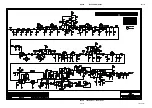
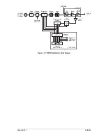
(Refer to Figure 2.3.)
The synthesiser employs a phase-locked loop (PLL) to lock a voltage controlled oscilla-
tor (VCO) to a given reference frequency. A reference oscillator at 12.8MHz (IC1) is buff-
ered (IC7c & b) and divided down to 200kHz (IC4). This 200kHz square wave is then
summed with the modulating audio and passed to an integrator (IC7f, Q8, Q9). This
produces a ramping waveform which is centred around a DC level determined by the
incoming audio. IC7e performs as a comparator, ultimately producing a phase-modu-
lated 200kHz square wave. This is followed by a similar phase shifting stage (IC7d & a,
Q10, Q11), before being divided down to 6.25kHz or 5kHz within the synthesiser IC
(IC5).
A buffered output of the VCO is divided with a programmable divider, comprising a
VHF prescaler (IC3) and a divider within IC5. This signal is compared with the phase
modulated reference signal at the phase detectors in IC5. A digital phase detector (PDB)
provides rapid coarse tuning of the VCO until the phase error is within the range of the
high gain sample and hold detector (PDA). The phase detector outputs are passed
through an active loop filter (IC6) which produces a DC voltage between 0V and 20V to
tune the VCO. This VCO control line is further filtered to attenuate noise and other spu-
rious signals. Note that the VCO frequency increases with increasing control voltage.
If the synthesiser loop loses lock, a pulsed signal appears at LD (pin 3) of IC5. This sig-
nal is filtered and buffered by IC6, producing the lock detect signal used to shut off the
power supply to the drive amplifier.
The division ratio of the programmable divider is stored within EPROM memory. Up to
128 frequencies can be stored within the EPROM and are addressed using the internal
DIP switches. Three of the address lines are also available for external frequency control
via an extra D-range connector at the rear of the chassis. A change of state of any of
these three lines commences a programming cycle, during which time the frequency
data in the EPROM is down loaded to the divider (IC5). 32 bits of data are loaded in
eight 4-bit words.
Note that the three address lines must change their state decisively and simultaneously.
Methods which allow the states of the three lines during transition to be undefined for
indeterminate lengths of time, as with some mechanical BCD switches, are unsuitable.
Summary of Contents for T830 Series
Page 10: ...31 01 96 Copyright TEL...
Page 12: ...31 01 96 Copyright TEL...
Page 16: ...31 01 96 Copyright TEL...
Page 20: ...31 01 96 Copyright TEL...
Page 22: ...31 01 96 Copyright TEL...
Page 24: ...31 01 96 Copyright TEL...
Page 28: ...31 01 96 Copyright TEL...
Page 30: ...31 01 96 Copyright TEL...
Page 32: ...31 01 96 Copyright TEL...
Page 38: ...31 01 96 Copyright TEL...
Page 40: ...31 01 96 Copyright TEL...
Page 62: ...31 01 96 Copyright TEL...
Page 68: ...31 01 96 Copyright TEL...
Page 70: ...31 01 96 Copyright TEL...
Page 84: ...31 01 96 Copyright TEL...
Page 88: ...31 01 96 Copyright TEL...
Page 94: ...31 01 96 Copyright TEL...
Page 98: ...31 01 96 Copyright TEL...
Page 108: ...31 01 96 Copyright TEL...
Page 110: ...31 01 96 Copyright TEL...
Page 116: ...31 01 96 Copyright TEL...
Page 118: ...31 01 96 Copyright TEL...
Page 140: ...31 01 96 Copyright TEL...
Page 142: ...31 01 96 Copyright TEL...
Page 148: ...31 01 96 Copyright TEL...
Page 160: ...31 01 96 Copyright TEL...
Page 162: ...31 01 96 Copyright TEL...
Page 166: ...31 01 96 Copyright TEL...
Page 172: ...31 01 96 Copyright TEL...
Page 180: ...31 01 96 Copyright TEL...
Page 190: ...31 01 96 Copyright TEL...
Page 192: ...31 01 96 Copyright TEL...
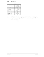
Page 196: ...31 01 96 Copyright TEL 1 3 Versions Description Version 10 136 174MHz...
Page 198: ...31 01 96 Copyright TEL...
Page 204: ...31 01 96 Copyright TEL...
Page 212: ...31 01 96 Copyright TEL...
Page 218: ...31 01 96 Copyright TEL...
Page 220: ...31 01 96 Copyright TEL...
Page 222: ...31 01 96 Copyright TEL...
Page 224: ...31 01 96 Copyright TEL...
Page 228: ...31 01 96 Copyright TEL...
Page 232: ...31 01 96 Copyright TEL...
Page 236: ...31 01 96 Copyright TEL...
Page 238: ...31 01 96 Copyright TEL...
Page 240: ...31 01 96 Copyright TEL...
Page 243: ...T800 Memory PCB IPN 220 01144 00 Top Side Copyright TEL 31 01 96...
Page 244: ...31 01 96 Copyright TEL T800 Memory PCB IPN 220 01144 00 Bottom Side...
Page 246: ...E2 6 T800 Memory PCB Information M830 00 31 01 96 Copyright TEL...
Page 250: ...31 01 96 Copyright TEL...
Page 251: ...T830 VCO PCB IPN 220 01176 01 Bottom Side Copyright TEL 31 01 96...
Page 252: ...31 01 96 Copyright TEL T830 VCO PCB IPN 220 01176 01 Top Side...
Page 253: ...M830 00 T830 VCO PCB Information E3 7 Copyright TEL 31 01 96 T830 VCO 220 01176 01...
Page 254: ...E3 8 T830 VCO PCB Information M830 00 31 01 96 Copyright TEL...
Page 256: ...31 01 96 Copyright TEL...
Page 260: ...31 01 96 Copyright TEL...
Page 264: ...31 01 96 Copyright TEL...
Page 272: ...31 01 96 Copyright TEL...
Page 278: ...31 01 96 Copyright TEL...
Page 284: ...31 01 96 Copyright TEL...

