background image

22

Description

TM8100/TM8200 Service Manual

© Tait Electronics Limited


June 2006

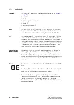
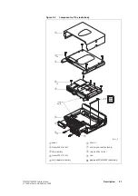
The front of the chassis has an aperture for the control-head connector. 
The control-head seal is fitted inside a groove around the flange at the front 
face of the chassis and provides for IP54 class protection when the control 
head is fitted. Two dot-dash-dot marks at the underside side of the chassis 
indicate the leverage points for removing the control head from the 
radio body.

The sides of the chassis contain two of the four screw bosses to attach the 
radio to the U-bracket of the installation kit.

For heat dissipation, the chassis has heat fins at the rear, grooves at the 
bottom, and holes in the front. 

The heat fins at the rear of the 40W/50W radio are longer than those of the 
25W radio. The grooves at the bottom of the 40W/50W radio are deeper 
than those of the 25W radio.

For additional heat dissipation, the 40W/50W radio has an additional 
L-shaped gap pad 

1)

 between the chassis and the main board.

Summary of Contents for TM8235

Page 1: ...TM8100 mobiles TM8200 mobiles Service Manual MMA 00005 04 Issue 4 June 2006...

Page 2: ...urisdictions Enquiries and Comments If you have any enquiries regarding this manual or any comments suggestions and notifications of errors please contact Technical Support Updates of Manual and Equip...

Page 3: ...10 Receiver Fault Finding 239 11 Transmitter Fault Finding 40W 50W 259 12 Transmitter Fault Finding 25W 323 13 CODEC and Audio Fault Finding 381 14 Fault Finding of Control Head with Graphical Display...

Page 4: ...04 05 Ignition Sense Kit 549 29 TMAA10 01 Desktop Microphone 551 30 TMAA10 02 Handset 555 31 TMAA10 03 and TMAA10 06 High Power Remote Speakers 559 32 TMAA10 04 Remote PTT Kit and TMAA10 05 Hands Free...

Page 5: ...numbers of the boards are listed below the last two digits in the IPN represent the issue of the board The board information in this manual covers all production issue boards up to the issue listed be...

Page 6: ...in Board B1 50W MMA 00021 xx TM8100 TM8200 Main Board H5 H7 40W MMA 00035 xx TM8100 Control Head Board 2 Digit Display MMA 00036 xx TM8100 Control Head Board 1 Digit Display MMA 00015 xx TM8200 Contro...

Page 7: ...g This alert is used when there is a potential risk of death or serious injury Caution This alert is used when there is the risk of minor or moderate injury to people Important This alert is used to w...

Page 8: ...on CTCSS Continuous Tone Controlled Subaudible Signaling DAC Digital to Analog Converter DC Direct Current DSP Digital Signal Processor DTMF Dual Tone Multi Frequency EPTT External PTT Press To Talk E...

Page 9: ...nit PTT Press To Talk RISC Reduced Instruction Set Computing RSSI Received Signal Strength Indication SFE Software Feature Enabler SMA Sub Miniature Version A SMD Surface Mount Device SMT Surface Moun...

Page 10: ...10 TM8100 TM8200 Service Manual Tait Electronics Limited June 2006...

Page 11: ...TM8100 TM8200 Service Manual 11 Tait Electronics Limited June 2006 TM8100 mobiles TM8200 mobiles Chapter 1 Description of the Radio...

Page 12: ...onnectors 36 2 4 Hardware and Software Architecture 45 2 5 Operation in Receive Mode 50 2 6 Operation in Transmit Mode 55 3 Circuit Descriptions 63 3 1 Transmitter Circuitry 65 3 2 Receiver Circuitry...

Page 13: ...remote monitoring and similar applications This manual includes the information required for servicing the radio and its accessories This section describes the different options available for frequen...

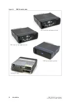
Page 14: ...ervice Manual Tait Electronics Limited June 2006 Figure 1 2 TM8100 mobile radios rear view 25W radio TM8115 radio with 2 digit display control head TM8110 radio with 1 digit display control head TM810...

Page 15: ...e radio body The control heads are identical for all frequency bands 1 2 RF Output Power The radio bodies are available with 40W 50W and 25W RF output power The two RF output power options are impleme...

Page 16: ...tion kit including a U bracket Installation of the radio is described in the user s guide or the installation guide Optional installation kits are remote control head kit for remote installation of th...

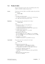
Page 17: ...fies the digital boards of the digital TM9100 product line c identifies the RF output power 2 25W 3 25W trigger base 4 30 to 59W 5 30 to 59W trigger base dd identifies the frequency band A4 66 to 88MH...

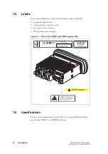
Page 18: ...rning 1 6 Specifications For up to date specifications refer to the area on the TaitWorld website reserved for TM8100 and TM8200 products Figure 1 3 Labels of the TM8100 and TM8200 product lines Conta...

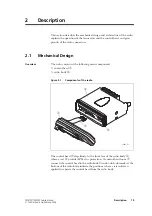
Page 19: ...Design Overview The radio consists of the following main components control head B radio body C The control head B clips firmly to the front face of the radio body C where a seal E provides IP54 class...

Page 20: ...ur screw bosses to attach the radio to the U bracket of the installation kit Internal Options Board Optional On the inside of the lid nine screw points are provided for mounting an internal options bo...

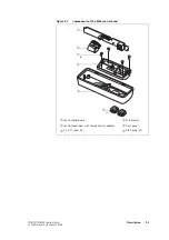
Page 21: ...June 2006 Figure 2 2 Components of the radio body B cover G chassis C screw M4x16 x4 H auxiliary connector bung D lid assembly I screws M4x16 x2 E screw M3x10 x5 J seal F main board assembly 1 gap pad...

Page 22: ...e leverage points for removing the control head from the radio body The sides of the chassis contain two of the four screw bosses to attach the radio to the U bracket of the installation kit For heat...

Page 23: ...ear of the radio body Figure 2 3 Components of the main board assembly B M3x10 screw x3 J D range screwlock fastener x2 C 50W 40W radios M2 2x10 PT screw x2 25W radios K30x8 PT screw x2 1 power connec...

Page 24: ...io and the auxiliary F power 1 and RF 1 connectors facing the rear of the radio are located on the bottom side of the main board The 40W 50W radio has a black power connector 1 and the 25W radio has a...

Page 25: ...ssembly with self adhesive coating and can be replaced for rebranding purposes Three clips on the rear side of the front panel assembly snap onto the space frame to hold the keypads 1 and 1 the LCD as...

Page 26: ...to the microphone The hole is covered by the rubber seal to ensure that the control head remains sealed to IP54 standards For more information refer to TMAA02 07 Concealed Microphone on page 501 Spac...

Page 27: ...D control head loom assembly with female female adapter E 3 x 10 PT screw x4 F control head board G space frame seal x2 H short light pipe I long light pipe J space frame 1 speaker clamp 1 speaker 1...

Page 28: ...the optional concealed microphone The side facing the front panel has the volume control potentiometer the microphone connector the indicator and backlight LEDS and the contacts for the keypads Contro...

Page 29: ...oses Six clips on the space frame G snap into corresponding locations on the inside of the front panel assembly to hold the keypad 1 the LCD 1 and the speaker J in place Knob for Volume Control Potent...

Page 30: ...at the same time allows access to their electrical contacts The rear side of the space frame has three holes for the screws D of the control head board E Control Head Board The control head board E is...

Page 31: ...h female female adapter I knob for volume control potentiometer C control head options board optional J speaker D 3 x 8 PT screw x3 1 concealed microphone optional E control head board 1 LCD F elastom...

Page 32: ...front panel with self adhesive coating and can be replaced for rebranding purposes The rear side of the front panel has four screw bosses to fasten the PCB bracket E Control Head Loom The control head...

Page 33: ...ion 33 Tait Electronics Limited June 2006 Figure 2 7 Components of the RJ45 control head B control head board E PCB bracket C control head loom with female female adapter F front panel D 3 x 8 PT scre...

Page 34: ...l Head Loom The programming connector at one end of the control head loom and a foam seal F are screwed to the front panel with a pair of lock nuts D When the programming connector is not in use the s...

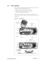
Page 35: ...to both short and long key presses A short key press is less than one second and a long key press is more than one second Figure 2 9 User interfaces scroll keys on off key volume control microphone so...

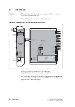
Page 36: ...board and the internal connectors of the control head refer to the PCB information of the main boards and the control head board Figure 2 10 Connectors radio with graphical display control head Speake...

Page 37: ...d June 2006 Figure 2 11 Connectors of the radio body 25W radio control head connector provision for external options connector provision for additional connector power connector auxiliary connector RF...

Page 38: ...al display Figure 2 13 Connectors of the control head with 1 2 or 3 digit display front view rear view without adapter flange microphone connector control head connector front view microphone connecto...

Page 39: ...nnectors for the 40W 50W and 25W radios Important The speaker load configuration is balanced the speaker output lines must not be connected to ground Connecting a speaker output line to ground will ca...

Page 40: ...ense input a Digital 3V3 CMOS 4 AUX_GPI3 General purpose digital input Programmable function With LK2 fitted GPI3 is a power sense input a Digital 3V3 CMOS 10 AUX_GPIO4 Programmable function and direc...

Page 41: ...al options connector pins and signals Pinout Pin Signal Description Signal type 1 13V8_SWa Switched 13V8 supply Supply is switched off when the Radio Body is switched off Power 2 AUD_TAP_OUT Programma...

Page 42: ...g ground Ground 7 CH_RXD Asynchronous serial port Receive data Digital 3V3 CMOS 8 DGND Digital ground Ground 9 CH_ON_OFF Hardware power on software controlled power off input Active low Digital 10 VOL...

Page 43: ...ut from microphone Also carries hookswitch signal Digital 5 MIC_AUD Fist microphone audio input Analog 6 AGND Analog ground Analog ground 7 MIC_RXD Asynchronous serial port Receive data 3 3V CMOS 8 MI...

Page 44: ...gnal type 1 PRG_RX_AUD Receive audio output Analog 2 PRG_TXD Asynchronous serial port Transmit data 3 3V CMOS 3 PRG_MIC_AUD Fist microphone audio input Analog 4 PRG_RXD Asynchronous serial port Receiv...

Page 45: ...oard has an internal options connector which allows internal options boards to access a variety of discrete and programmable signals For more information refer to Internal Options Connector on page 41...

Page 46: ...Interface Digital Board RF Connector Power Connector Control Head Connector LPF 1 PIN Switch 1 Auxiliary Connector Internal Options Connector Main Board FPGA RISC Proc Serial Flash SRAM Flash Memory p...

Page 47: ...oftware modules are stored on the digital board of the main board FPGA image which includes the software implemented RISC processor and the custom logic the custom logic executes additional digital si...

Page 48: ...n the control head 3 Normal radio operation starts with the RISC processor executing the radio application code including application software the DSP executing the DSP code for processing of digital...

Page 49: ...which is part of the radio and control head application software Software Shutdown On shutdown the programming and calibration data is stored in the database and power is removed from the radio Impor...

Page 50: ...transceiver is illustrated in Figure 2 16 on page 51 These block diagrams show the hardware modules integrated with the software modules hardware transmitter receiver CODEC and audio RISC processor o...

Page 51: ...oint Equalization Audio Filtering Pre emphasis Optional Processing Data and Signaling Encoders ALC Dir Coup Fin Drv Ex Pwr Ctrl Ramp Control TCXO 13 000 MHz VCO Control Head VCXO Bias Custom Logic Har...

Page 52: ...64kHz The quadrature output from this mixer is fed to a pair of ADCs with high dynamic range where it is oversampled at 256kHz and fed to the custom logic device Automatic Gain Control The AGC is use...

Page 53: ...and fed via a single synchronous serial port to the DSP The stream is demultiplexed and the demodulation data used as an input for further audio processing Noise Squelch The noise squelch process resi...

Page 54: ...in the order of 10dB relative to full scale in the receive path CODEC The combined audio and side tone signal is converted to analog form by a 16 bit DAC with integral anti alias filtering This is fol...

Page 55: ...transceiver is illustrated in Figure 2 16 on page 51 These block diagrams show the hardware modules integrated with the software modules hardware transmitter receiver CODEC and audio RISC processor on...

Page 56: ...atic Level Control The ALC follows and is used to effectively increase dynamic range by boosting the gain of the microphone pre amplifier under quiet conditions and reducing the gain under noisy acous...

Page 57: ...ties Note that patents are pending for several aspects of the synthesizer design Operation of Control Loop The RF PLL is a conventional integer N type design with frequency resolution of 25kHz In tran...

Page 58: ...DC Reference modulation is usually applied directly to the TCXO In the system employed in the radio the frequency reference is generated by the FCL which itself requires dual point modulation injectio...

Page 59: ...6 3 RF Transmitter RF Power Amplifier and Switching 50W 40W Radio The RF power amplifier and exciter of the 40W 50W radio is a five stage line up with approximately 40dB of power gain The output of th...

Page 60: ...djacent channel power A typical ramping waveform is shown in Figure 2 17 Bias Ramp Up The steady state final stage bias level is supplied by an 8 bit DAC programmed prior to ramp up but held to zero b...

Page 61: ...m shape remains the same for all power levels PIN Switch The RF PIN switch circuitry selects the RF path to and from the antenna to either the Tx or Rx circuitry of the radio In addition to the switch...

Page 62: ...62 Description TM8100 TM8200 Service Manual Tait Electronics Limited June 2006...

Page 63: ...rds The main board is divided into the following circuitry modules transmitter receiver frequency synthesizer including FCL CODEC and audio power supply interface digital board Figure 3 1 gives an ove...

Page 64: ...Interface Digital Board RF Connector Power Connector Control Head Connector LPF 1 PIN Switch 1 Auxiliary Connector Internal Options Connector Main Board FPGA RISC Proc Serial Flash SRAM Flash Memory...

Page 65: ...The power amplifier comprises the driver amplifier Q306 and two paralleled final devices Q309 and Q310 With the 40W 50W radio the signal from the exciter is amplified by Q306 to a power level of appro...

Page 66: ...er and Level Shifter Crowbar Shaping Filter Tempera ture Sensor Buffer Amplifier TX RX RF Thermal Coupling OR Gate Switch TX INH 9V0 TX 13V8 BATT DIG TX INH DIG SYN EN SYN LOCK SYN TX LO Power Supply...

Page 67: ...power control loop senses the forward power by means of the diode D304 This signal is fed to the buffer and a band limited operational amplifier back to the gate of Q306 A voltage clamp one of the ope...

Page 68: ...mmed First IF Stage and Second Mixer The first IF stage consists of a crystal channel filter BPF1 followed by an IF amplifier and then another crystal filter BPF2 The second mixer is an IC quadrature...

Page 69: ...TURE DEMODULATOR BIAS NETWORK POWER SUPPLY CODEC AND AUDIO CIRCUITRY DIGITAL BOARD PLL TRANSMITTER FREQUENCY SYNTHESIZER MIXER RF SIGNAL TYPES ANALOGUE CLOCK DIGITAL ASYNCHRONOUS SERIAL DATA SYNCHRONO...

Page 70: ...rk Power Supply CODEC and Audio Digital Board PLL Noise Blanker 66 174 MHz only Switch 66 225 MHz only Transmitter Frequency Synthesizer Mixer Receiver VCO CDC RX PIN AGC CDC RX AGC RX CDC QN RX CDC Q...

Page 71: ...inimizing distortion Received Signal Strength Indication The RSSI is calculated in the FPGA and DSP and can be passed as an analog voltage to the internal options interface and the external auxiliary...

Page 72: ...regulator output voltage is electrically noisy however and filtering is essential Filtering of the power supply is achieved with two capacitance multipliers Q508 and C585 for the VCO supply and Q512...

Page 73: ...fier PLL MOD VCO 2 VCO 1 Buffer Amplifiers and Coupler 5 V Switch TR Switch VCO UHF only 6V0 AGND 3V0 AN Power Supply CDC VCXO MOD SYN CDC FCL SYN CDC LFV CDC VCO MOD CODEC and Audio SYN TX LO SYN RX...

Page 74: ...mode the output power should be about 7dBm whereas in transmit mode it should be about 9dBm Dual VCOs Some variants of the synthesizer use two VCOs one for receive and one for transmit Synthesizers wi...

Page 75: ...re tuned is dependent on many factors of which the loop filter is the main factor The loop filter is an integrator built around an operational amplifier The resistors and capacitors of the filter affe...

Page 76: ...rcuit Operation The VCXO is mixed with the TCXO output to create a nominal difference or offset frequency of 12kHz SYN CDC FCL In A4 band radios there is additional circuitry and the VCXO is mixed wit...

Page 77: ...I and Q outputs IRXP IRXN QRXP and QRXN balls of the receiver s second IF stage The analog signals are differential and biased at 1 2V nominally The digital section communicates with this CODEC via a...

Page 78: ...C FCL Digital Board AGND 13V8 BATT 2V5 CDC 9V0 3V3 3V0 AN CDC RX AUD AUD ITF SPK AUD ITF SPK ITF RX BEEP IN ITF CH MIC AUD ITF AUX MIC AUD ITF VOL WIP DC CDC AUD TAP OUT CDC RSSI ITF AUD TAP IN CDC2 D...

Page 79: ...C209 C211 R252 and R253 ensure stability of the amplifier at high frequencies When operational the output bias voltage for IC202 is approximately half the radio supply voltage When not operational the...

Page 80: ...lter formed by IC201 pins 1 to 3 R219 R220 R221 R224 C206 C208 and C210 is a third order Butterworth type with a cut frequency of approximately 12kHz The output of the low pass filter is amplified by...

Page 81: ...o 16V Supervisory Circuit The supervisory circuit comprises a reset and watchdog timer The circuit provides the reset signal PSU SYS RST to the digital section which in turn provides the watchdog sign...

Page 82: ...itch 3V3 2V5 Regulator 3 V Rx Switch PSU Super visor 13V8 Switch Reverse Polarity Protection 13V8 BATT 9V0 TX 9V0 3V0 AN 13V8 BATT 9V0 3V0 AN 3V3 2V5 CDC 3V0 AN 3V0 RX DIG RX EN DIG TX EN DIG SLP EN 3...

Page 83: ...provides four hardware links LK1 to LK4 on the top side of the main board which can be configured to attain the power sense option desired Figure 3 9 shows a block diagram of the hardware links LK1 to...

Page 84: ...ff AUX GPI3 2 6V high active ignition sense tolerant to 3 3V 5V and 12V LK1 out Input line must be active highb LK4 out IOP GPIO7 can be used as GPIO internal power sense LK1 out IOP GPIO7 0 7V off IO...

Page 85: ...cle installation this avoids flattening the battery when the ignition key is off Internal Options Power Sense This option is similar to the auxiliary power sense option except that the IOP GPIO7 line...

Page 86: ...will always be supplied to the connector while the primary power source is connected to the radio and is alive The supply to the connector is not affected by the state of the radio Switched power mean...

Page 87: ...s a small voltage drop across R761 causing the collector emitter to saturate As the collector current increases the base current decreases proportionally until the voltage across R761 reaches 1V At th...

Page 88: ...V3 AGND DGND SPK SPK VOL WIP DC CH MIC AUD RX AUD CH ON OFF CH RXD CH TXD CH PTT CH GPIO1 CH SPI DI CH SPI DO CH SPI CLK CH LE RX AUD RX BEEP IN AUD TAP OUT AUD TAP IN AUX MIC AUD RSSI 13V8 SW IOP GPI...

Page 89: ...ly a dedicated ignition sense input but can be made a general purpose input like AUX GPI1 by removing the link LK2 in the power supply area and fitting the 33k resistor R775 ESD Protection On exposed...

Page 90: ...DIG CH SPI CLK DIG CH SPI DO ITF CH SPI DI DIG CH LE ITF CH GPI1 DIG CH GPO1 ITF CH PTT ITF CH HOOK ITF ON OFF ITF IOP GPIO1 7 DIG IOP TXD ITF IOP RXD ITF AUX GPI1 7 DIG AUX GPO4 7 DIG AUX TXD ITF AU...

Page 91: ...l EEPROM DGND AGND DIG CH SPI CLK DIG CH SPI DO ITF CH SPI DI DIG CH LE ITF CH GPI1 DIG CH GPO1 ITF CH PTT ITF CH HOOK ITF ON OFF ITF IOP GPIO1 7 DIG IOP TXD ITF IOP RXD ITF AUX GPI1 7 DIG AUX GPO4 7...

Page 92: ...or function keys F1 and F4 keypad backlighting LEDs speaker Connectors The control head board includes the circuitry for the following connectors microphone connector RJ45 socket control head connecto...

Page 93: ...UART JTAG 3V3 Soldering Pads AGND DGND Concealed Microphone Speaker MIC MIC AGND Power Supply 3V3 1V5 1V5 3V3 13V8 CH RXD CH TXD CH GPIO1 CH PTT CH ON OFF 13V8 SPK SPK SPK SPK Speaker Leads Microphon...

Page 94: ...e each from the FPGA which switch two transistors on MOSFET Q102 A temperature signal from the LCD module is converted to a digital signal by an analog digital converter U601 and processed by the FPGA...

Page 95: ...cealed microphone two control head options connectors for optional circuit board Protection circuitry is provided for the microphone connector For pinouts of the control head connector and the microph...

Page 96: ...3V3 13V8 SW CH ON OFF CH SPI DI CH LE CH SPI CLK 3V3 AGND DGND Contact made when key pressed Contact made when key pressed Speaker Leads SPK SPK 13V8 SW MIC AUD IN P1 MIC AUD OUT DGND AGND VOL WIP DC...

Page 97: ...een clocked in the latch line is driven low On this falling edge all the outputs LEDs and LCD segments are driven to their new state When the latch line is driven high the state of each key is latched...

Page 98: ...ts of the connectors refer to Connectors on page 36 Basic Circuitry The signals of the control head connector are directly connected to the telemetry connector The POWER ON OFF LED is supplied by the...

Page 99: ...TM8100 TM8200 Service Manual 99 Tait Electronics Limited June 2006 TM8100 mobiles TM8200 mobiles Chapter 2 Servicing the Radio...

Page 100: ...moving and Mounting the Control Head 130 5 2 Disassembling the Radio Body 131 5 3 Reassembling the Radio Body 137 5 4 Disassembling and Reassembling the Control Head 141 6 Servicing Procedures 149 6 1...

Page 101: ...wer 332 12 3 Biasing of PA Driver and PAs 342 12 4 RF Signal Path 361 13 CODEC and Audio Fault Finding 381 13 1 Power Supplies 382 13 2 Faulty Speaker Audio 384 13 3 No Speaker Audio at Auxiliary Conn...

Page 102: ...ead with 1 2 or 3 Digit Display 429 15 1 Display Faulty but not LEDs 432 15 2 Some LEDs Faulty 433 15 3 All LEDs Faulty 434 15 4 Display and All LEDs Faulty 434 15 5 Some but not All Keys Faulty 435 1...

Page 103: ...ors on the main board assembly however are level 2 repairs because these repairs entail the disassembly of the main board assembly Important The circuit boards in the radio are complex They should be...

Page 104: ...vel 2 repairs ASC and Tait only access Log in passwords are needed for associate and Tait only access Technical Support supplies service centres with the necessary log in information The unsecured por...

Page 105: ...in the layout of the board All PCB information is published on the Technical Support website Tait FOCUS Database An additional source of information to service centres is the Tait FOCUS call logging...

Page 106: ...ay be used instead However it should be noted that a hot air tool affords little control Even in skilled hands use of a hot air tool to remove cans will result in rapid uncontrolled rises in the tempe...

Page 107: ...0 04 cable listed is required only if the test PC is to be connected directly to the radio for programming purposes Note The characters xx below stand for the issue number of the manual Only the lates...

Page 108: ...of the bench when disassembling and re assembling the radio Compliance Issues Note The radio is designed to satisfy the applicable compliance regula tions Do not make modifications or changes to the r...

Page 109: ...er s instructions A typical installation is shown in Figure 4 1 These benches have a dissipative rubber bench top a conductive wrist strap and a connection to the building earth The material of the be...

Page 110: ...at transfer block must be secured to the main board The lid of the radio body may be left off After completing any measurement or test requiring activation of the transmitter immediately return the ra...

Page 111: ...espectively the switches of the test unit must be set as described below When programming or calibrating radios the switches have no effect although it is good practice to set the MODE switch to RX Se...

Page 112: ...AD connector BNC transmit audio connector BNC computer connector RJ12 serial port DB9 speaker connector banana plugs AC input BNC audio monitor out BNC AUDIO IN HI BNC AUDIO OUT BNC RF in out N type p...

Page 113: ...CB information for the board consult the parts list for the board Identify the component in question in the parts list Note however that a new PCB information is published only whenever there is a maj...

Page 114: ...e main board assembly are identified in Figure 4 3 and Figure 4 4 The figures also show the locations of the connectors on the board Figure 4 3 Shielding cans and connectors top side of main board ass...

Page 115: ...icians should refer to the documentation supplied with the tool for the correct procedures If the tool is not available a hot air tool may be used instead However technicians require training in the b...

Page 116: ...ard techniques and these are discussed below Another issue of concern is the procedure for removing and installing cans A discussion of the issue concludes this section Non standard Procedures Do not...

Page 117: ...Limited June 2006 Figure 4 5 Locations of the capacitors C548 and C565 and the inductors L601 and L602 top side VHF board UHF board similar Note that other components may be fitted for C548 such as C...

Page 118: ...ry first select the settings for the communications port as follows 1 Open the terminal program In the case of HyperTerminal click Start Programs Accessories Communications HyperTerminal 2 In the term...

Page 119: ...speaker 74 x where x is the required state 0 stand by 1 on 2 mute None 110 Audio volume Sets the level of the audio volume 110 x where x defines the required level any integer from 0 to 255 None 138...

Page 120: ...character identifier and y is an eight digit version number 133 Hardware version Reads the product code of the radio body and the hardware version number 133 x y where x is the product code and y is t...

Page 121: ...sage with results of calibration attempt 334 Synthesizer power Switches the frequency synthesizer on or off via the DIG SYN EN line 334 x where x is the required state 0 off 1 on None 335 Synthesizer...

Page 122: ...from 0 to 1023 114 x to set value where x is the required power setting an integer from 0 to 1023 None 304 Driver bias Sets or reads the clamp current at the gate of the PA driver 304 to read value x...

Page 123: ...r the first PA 331 to read value x where x is the DAC value of the bias voltage an integer from 0 to 255 331 x to set value where x is the DAC value of the required bias voltage any integer from 0 to...

Page 124: ...e elements of the display on or off 1006 x where x is the required state 0 off 1 on None 1007 LCD temperature sensor Reads the output of the LCD temperature sensor 1007 x where x corresponds to the te...

Page 125: ...own and up again and place the radio in CCTM again C05 The radio has not responded within the specified time Re enter the CCTM command X04 The DSP is not responding Check the DSP pin connections If th...

Page 126: ...uency or identified by the frequency sub band such as B1 or H7 For example The frequency bands for TM8100 TM8200 radios are listed in Table 4 11 The relevant frequencies for the different bands are li...

Page 127: ...le 6 1 on page 154 Audible indications are provided in the form of different tones emitted from the speaker The information conveyed by the tones is given in Table 4 13 on page 128 Table 4 12 Visual i...

Page 128: ...cepted and radio is ready to use 3 After radio has been stunned Radio has been revived and is ready to use Two low pitched beeps While powered up Temperature of radio is high Two high pitched beeps Wh...

Page 129: ...ody disassemble and reassemble the control heads General Important Before disassembling the radio disconnect the radio from any test equipment or power supply Disassemble only as much as necessary to...

Page 130: ...rtant When inserting the flat bladed screwdriver take care not to damage the control head seal 3 At either of the lever points insert a 3 16 inch 5mm flat bladed screwdriver between the control head a...

Page 131: ...ctions refer to Reassembling the Radio Body on page 137 Removing the Cover 1 At the upper edge of the lower screw bosses on both sides of the radio body insert a 1 8 inch 3mm flat bladed screwdriver 2...

Page 132: ...ing one of the tabs located at the bottom of the seal preferably by hand If necessary lift up the tap using the blade of a small flat bladed screwdriver Do not damage the seal with the screwdriver 3 U...

Page 133: ...the radio body B cover G chassis C screw M4x16 x4 H auxiliary connector bung D lid assembly I screws M4x16 x2 E screw M3x10 x5 J RF connector seal F main board assembly 1 gap pad 50W 40W radio only T...

Page 134: ...screws b securing the main board 1 to the heat transfer block F Note Make sure not to touch the thermal paste on the heat transfer block and the underside side of the main board If the thermal paste...

Page 135: ...os K30x8 PT screw x2 I power connector seal J power connector 1 gap pad 50W 40W radio only D auxiliary connector 1 RF connector nut E inner foam D range seal 1 RF connector lock washer F heat transfer...

Page 136: ...cap c if fitted Undo the two D range screwlock fasteners d 2 Undo up to nine screws h and remove the options board G from the lid assembly E 3 If an external options connector is fitted a foam seal fo...

Page 137: ...rews C to 3lb in 0 34N m 2 If the outer foam seal E or the inner foam D range seal G have been removed fit new seals to the heat transfer block F 3 With the 40W 50W radio the rectangular gap pad 1 mus...

Page 138: ...o Figure 5 6 on page 137 5 Place the main board 1 in position on the heat transfer block F and push them together to spread the thermal paste Important You must observe the following order of assembly...

Page 139: ...the L shaped ridge of the chassis Peel off the transparent film on other of the gap pad 2 If the thermal paste on the heat transfer block or the underside of the main board has been contaminated new t...

Page 140: ...connector seal j Ensure that the seal is properly seated around its entire periphery 9 If an auxiliary connector bung h was fitted fit the bung Closing the Radio Body The circled number in this sectio...

Page 141: ...lange C 3 Disconnect the control head loom D 4 If an optional circuit board is fitted unplug it from the control head board F refer to Figure 5 8 5 Note whether the speaker is connected or disconnecte...

Page 142: ...spaceframe and remove it along with the two seals G Check the seals G and replace them if necessary 11 Remove the speaker 1 and speaker clamp 1 Important When fitting the speaker and the speaker clam...

Page 143: ...with female female adapter E 3 x 10 PT screw x4 F control head board G space frame seal x2 H short light pipe I long light pipe J space frame 1 speaker clamp 1 speaker 1 LCD assembly including LCD se...

Page 144: ...rol head board refer to Figure 5 10 Note that the radio must be returned to the customer in its original configuration 5 Use a Torx T10 screwdriver to unscrew the three screws D securing the control h...

Page 145: ...he concealed microphone 1 Important When replacing the LCD carefully remove the protective plastic film from the LCD Take care not to scratch the soft polarizer material on the top side of the LCD Fig...

Page 146: ...refer to the items in Figure 5 12 1 Release the clip of the PCB bracket E and remove the control head board B 2 Disconnect the control head loom C from the control head board B 3 Use a Torx T10 screw...

Page 147: ...screws B and remove the cover seal Note that the radio must be returned to the customer in its original configuration 2 Note whether an options board not shown is fitted inside the control head If a a...

Page 148: ...148 Disassembly and Reassembly TM8100 TM8200 Service Manual Tait Electronics Limited June 2006...

Page 149: ...file checking the user interface checking any error messages The following tasks only need to be carried out if they relate to the fault reported checking the transmit and transmit audio functions ch...

Page 150: ...t the upper part of the seal and then press down around the sides of the seal to the bottom Ensure that the seal is properly seated around its entire periphery Check for Additional Damage Also check f...

Page 151: ...the radio powers up successfully go to Task 4 If it does not go to Step 3 3 Check the fuses cables and the power supply 4 Check whether the control head loom the control head or the radio body is fau...

Page 152: ...Refer to the troubleshooting section of the online help 5 If the programming file can be read now save a copy on the test PC and go to Task 5 If not go to Step 6 6 Check whether the control head loom...

Page 153: ...tart up sequence the LEDs light up red briefly the speaker gives two short beeps LCD and keypad backlighting activates the LCD displays a power up message then a channel number or an error message 3 C...

Page 154: ...001 Unknown Turn the radio off and then back on Error E0002 Unknown Continue with servicing tasks to locate the problem Error E0003 Corrupt FW Re download the radio s firmware Error E0008 System error...

Page 155: ...se CCTM command 326 1 to set the power level to very low 7 Connect a power meter and measure the transmit power 8 If the carrier power is correct go to Step 10 If the carrier power is not correct try...

Page 156: ...requency set to the top of the band 5 Feed a signal without modulation on the receive channel at 47dBm Check for maximum RSSI using the indicator on the radio display graphical display the green statu...

Page 157: ...sembly This section describes the steps after completion of the fault diagnosis 1 Use the programming and calibration applications to load the pro gramming and calibration files read or set up in Init...

Page 158: ...g of the same software features as in the original assembly Proceed as follows 1 If it was possible to read the software features in Obtain the Details of the Software Feature Enabler SFE on page 153...

Page 159: ...that it is fully functional again The recommended tests are listed in Table 6 2 to Table 6 4 The calibration application can be used for many of these tests It is good practice to record the test resu...

Page 160: ...kHz deviation wide band 3 3 CTCSS continuous tone controlled subaudible signaling deviation Narrow band Medium band Wide band 250 to 350 Hz 500 to 560 Hz 580 to 680 Hz Table 6 3 Final tests of receive...

Page 161: ...Data communications Test 1200 baud data transmission standard Test Tait high speed data transmission if feature is enabled Direct connect GPS global positioning system Check that GPS poll returns corr...

Page 162: ...162 Servicing Procedures TM8100 TM8200 Service Manual Tait Electronics Limited June 2006...

Page 163: ...sk 6 check provision of external power Types of Fault Which of the above tasks are applicable depends on the nature of the fault Radio fails to power up The radio fails to power up immediately when po...

Page 164: ...page 149 If it does not go to Step 5 5 Check the digital power up signal at pin 5 of IC602 see Figure 7 1 the signal is active high namely when the voltage exceeds 2 0V DC Measure the voltage at pin 5...

Page 165: ...anual Power Supply Fault Finding 165 Tait Electronics Limited June 2006 Figure 7 1 Important components of the power supply circuitry bottom side including 3 3V regulator IC602 pin 7 pin 5 C603 C618 R...

Page 166: ...ting the supply or preventing the radio from powering up While keeping the ON OFF key depressed measure the supply at the 3V3 test point near the corner of the digital board see Figure 7 2 The voltage...

Page 167: ...If the fault remains the repair failed replace the board and go to Final Tasks on page 157 6 Reconnect the 13 8V supply Press the ON OFF key If the radio powers up return to Initial Tasks on page 149...

Page 168: ...e of the relevant regulator IC Repair any fault 2 If the regulator IC has been removed resolder it in position 3 Reconnect the 13 8 V supply and press the ON OFF key If the radio powers up or the corr...

Page 169: ...s power sense IOP GPIO7 auxiliary power sense AUX GPI3 emergency power sense AUX GPI2 4 For the first two lines confirm that the Power Sense Ignition option has been selected in the Action field and H...

Page 170: ...or PL100 Repair any fault and go to Step 5 2 For the auxiliary power sense option the link LK2 should be inserted see Figure 7 2 Connect 3 3V DC more than 2 6V to be precise from the power supply to t...

Page 171: ...igure 7 1 is high Remove the 3 3V supply and ground the IOP GPIO7 line to be precise the voltage on the line should be less than 0 6V If the power up signal is now low conclude with Step 5 If it is no...

Page 172: ...ernal power to any of these connectors first confirm the link settings required and then carry out the following procedure 1 With the radio powered up confirm that 13 8V DC is present at pin 3 of IC60...

Page 173: ...e enclosures In Figure 8 1 which shows part of the internal options connector as an example IOP GPIO7 is a connector signal and ITF IOP GPIO7 is an internal signal Types of Signals The connector and i...

Page 174: ...00 Service Manual Tait Electronics Limited June 2006 Figure 8 2 Components of the interface circuitry top side near the CDC TOP and IF TOP cans Figure 8 3 Components of the interface circuitry top sid...

Page 175: ...d mechanical shock or vibration or to a temperature change This might expose any intermittent contact in which case go to Step 3 3 If the expected signal is not present check whether the expected inte...

Page 176: ...176 Interface Fault Finding TM8100 TM8200 Service Manual Tait Electronics Limited June 2006 Figure 8 4 Components of the interface circuitry bottom side...

Page 177: ...they are not go to Step 8 7 The fault lies with the radio s internal circuitry If the power supply circuitry or the CODEC and audio circuitry is suspect continue with the fault diagnosis as in Power S...

Page 178: ...178 Interface Fault Finding TM8100 TM8200 Service Manual Tait Electronics Limited June 2006...

Page 179: ...118 Use an oscilloscope with a x10 probe for all voltage measurements required The signals should appear stable and clean Consider any noise or unidentified oscillations as evidence of a fault requir...

Page 180: ...checks of Task 1 and Task 2 respectively are required In the last case there are several symptoms these are listed below Frequency Bands Where test procedures or figures differ according to the frequ...

Page 181: ...zer To determine which is faulty calibrate the VCXO and the transmit VCO as described below Always calibrate the former first because the latter depends on the former 1 Place the radio in CCTM 2 Enter...

Page 182: ...ceive mode Go to Power Supplies on page 183 Task 2 Lock Status A lock error indicates that the frequency synthesizer FCL or second LO is out of lock To determine which is faulty check the lock status...

Page 183: ...V DC supply from 6 V regulator in PSU module 6V0 Task 5 5 V DC supply following filtering of 6 V supply 5V DEC Task 6 3 V DC supply from 3 V regulator in PSU module 3V0 AN The measurement points for d...

Page 184: ...e 2006 Figure 9 2 Synthesizer circuitry under the SYN TOP can and the 6 V regulator IC606 top side VHF bands UHF bands Measurement point on L506 pin not used Pin 5 5 pin device Q508 Q507 Q506 Q508 Q51...

Page 185: ...Task 4 If it is not go to Step 5 5 Check the 9 V supply at Q500 and R533 see Figure 9 3 6 If the voltage is correct go to Step 7 If it is not the 9V regulator IC601 is suspect go to Task 3 of Power Su...

Page 186: ...ynthesizer Fault Finding TM8100 TM8200 Service Manual Tait Electronics Limited June 2006 Figure 9 3 Synthesizer circuitry under the FCL TOP can top side A4 band PAD TOP can top side PCB VCXO BOT can b...

Page 187: ...lator IC601 is suspect go to Task 3 of Power Supply Fault Finding on page 168 4 If the input to the regulator IC606 is correct but not the output check IC606 see Figure 9 2 and the associated circuitr...

Page 188: ...188 Frequency Synthesizer Fault Finding TM8100 TM8200 Service Manual Tait Electronics Limited June 2006 Figure 9 4 Synthesizer circuitry under the SYN BOT can bottom side IC505 IC504 Q505 Q511...

Page 189: ...e 5V and transmit receive switches based on Q506 Q507 and Q508 pins 1 2 6 see Figure 9 2 Replace any suspect transistor Conclude with Step 6 5 With a VHF radio check for faults in the C multiplier and...

Page 190: ...190 Frequency Synthesizer Fault Finding TM8100 TM8200 Service Manual Tait Electronics Limited June 2006 Figure 9 5 Transmit receive switch components VHF bands Q5003 Q5002 Q5003 Q5002 SYN TOP A4 band...

Page 191: ...k the supply at L506 see Figure 9 2 The measurement point is the via shown in the figure 4 If the voltage is correct go to Step 5 If it is not the 3 V regulator IC603 is suspect go to Task 3 of Power...

Page 192: ...inputs and output are summarized in Figure 9 6 Task 7 Supply for Charge Pump First check the supply for the charge pump of the PLL 1 Measure the supply for the charge pump at pin 16 of IC503 see Figu...

Page 193: ...TER AT C565 TP503 JUNCTION OF R566 AND R570 TP503 JUNCTION OF R566 AND R570 SIGNAL TYPES RF ANALOG CLOCK DIGITAL PLL LOOP FILTER AND SUMMER FILTERING OF SUPPLY FOR PLL AND LOOP FILTER FCL VCO CIRCUITR...

Page 194: ...9 2 2 If the signal is correct go to Task 9 If it is not go to Step 3 3 Check IC503 see Figure 9 2 Replace IC503 if it is suspect 4 Determine if the fault has been removed If it has go to Final Tasks...

Page 195: ...he digital board 6 Enter the CCTM command 334 1 to switch on the synthesizer and measure the voltage at the via between R104 see Figure 9 7 and the digital board 7 If the voltages measured in Step 5 a...

Page 196: ...is correct go to Loop Filter on page 198 If it is not go to Step 4 4 Check for continuity between pin 14 of IC503 and the digital board via R568 see Figure 9 2 and L102 see Figure 9 7 5 If there is a...

Page 197: ...equency Synthesizer Fault Finding 197 Tait Electronics Limited June 2006 Figure 9 8 Synthesizer circuitry under the SYN TOP can top side VHF bands UHF bands Q512 Q512 Junction of C541 and R547 Junctio...

Page 198: ...see Figure 9 8 3 Using an oscilloscope proceed as follows to observe the voltage at C565 before and after grounding the junction between C541 and R547 see Figure 9 8 While holding the oscilloscope pr...

Page 199: ...a system error or a transmit fault the transmit VCO is suspect go to Transmit VCO and Related Circuitry UHF Radios on page 212 Task 13 Check Reference Voltage If the loop filter circuitry is suspect f...

Page 200: ...sk 15 3 Check IC504 IC505 Q511 see Figure 9 4 and associated components 4 Check the following components see Figure 9 8 Note On early issue boards C548 is fitted instead of these components 5 If a fau...

Page 201: ...between R105 and the digital board see Figure 9 7 The result should be 9 Enter the CCTM command 389 0 to set the mode to slow 10 Measure the voltage at the via between R105 and the digital board see F...

Page 202: ...ds C548 may be fitted instead of these components 5 Remove R566 and R570 see Figure 9 8 which provide a modulation path to the VCO s 6 Repeat the measurement of Step 1 7 If the correct result is now o...

Page 203: ...d related circuitry The minimum and maximum receive frequencies for the different UHF frequency bands are defined in Table 9 3 There are six aspects Task 17 check receive VCO Task 18 repair PLL feedba...

Page 204: ...RX PORT PIN 4 OF IC5100 PIN 4 OF IC5100 SIGNAL TYPES RF ANALOG CLOCK DIGITAL PLL LOOP FILTER AND SUMMER FILTERING OF SUPPLY FOR VCO CIRCUITRY FREQUENCY SYNTHESIZER PLL FEEDBACK LOOP VOLTAGE RECEIVE VC...

Page 205: ...he maximum given in Table 9 3 3 If the receive frequency measured in Step 2 is correct go to Step 4 If it is incorrect go to Task 19 but if no frequency is detected go to Task 20 4 Proceed as follows...

Page 206: ...r Fault Finding TM8100 TM8200 Service Manual Tait Electronics Limited June 2006 Figure 9 10 Synthesizer circuitry under the SYN TOP and VCO TOP cans UHF radio top side Tx port Junction of C541 and R54...

Page 207: ...9 10 2 Remove the VCO BOT can 3 Replace the components C567 R574 see Figure 9 11 and IC503 see Figure 9 10 4 Also check the second stage of the receive buffer amplifier based on IC5100 see Figure 9 11...

Page 208: ...heck the receive VCO The circuitry is based on Q504 see Figure 9 10 3 If a fault is found repair it and go to Step 4 If no fault is found go to Step 6 4 Repeat the frequency measurements in Step 2 and...

Page 209: ...0 2 Enter the CCTM command 335 0 to switch on the supply to the receive VCO 3 Measure the voltage at the first collector pin 3 of Q506 see Figure 9 10 The voltage should be 4 Enter the CCTM command 33...

Page 210: ...tage at the via between R103 and the digital board 6 If the voltages measured in Step 4 and Step 5 are correct go to Step 7 If they are not the digital board is faulty resolder R103 in position see Fi...

Page 211: ...Enter the CCTM command 335 1 to set the transmit receive switch on 5 Again measure the voltages of Q5100 and IC5100 6 If the voltages are correct the receive VCO is suspect go to Step 7 If they are n...

Page 212: ...transmit VCO and related circuitry The minimum and maximum transmit frequencies for the different UHF frequency bands are defined in Table 9 4 There are five aspects Task 23 check transmit VCO Task 24...

Page 213: ...the maximum given in Table 9 4 3 If the transmit frequency measured in Step 2 is correct go to Step 4 If it is incorrect go to Task 25 If no frequency is detected go to Task 26 4 Proceed as follows to...

Page 214: ...the board and go to Final Tasks on page 157 Task 25 Repair Transmit VCO If either or both the minimum and maximum transmit frequencies are incorrect the transmit VCO circuitry is faulty 1 Remove the...

Page 215: ...0 2 Enter the CCTM command 335 1 to switch on the supply to the transmit VCO 3 Measure the voltage at the second collector pin 6 of Q506 see Figure 9 10 The voltage should be 4 Enter the CCTM command...

Page 216: ...eck the transmit buffer amplifier in transmit mode Enter the CCTM command 335 1 to set the transmit receive switch on 5 Again measure the voltage at Q5001 6 If the voltages are correct the transmit VC...

Page 217: ...dios the VHF frequency bands are defined in Table 9 5 There are six aspects Task 28 check VCO Task 29 repair PLL feedback Task 30 repair VCO Task 31 check transmit receive switch Task 32 repair switch...

Page 218: ...2 OF D5004 PIN 2 OF D5004 TX PORT TX PORT RX PORT RX PORT SIGNAL TYPES RF ANALOG CLOCK DIGITAL PLL LOOP FILTER AND SUMMER FILTERING OF SUPPLY FOR VCO CIRCUITRY FREQUENCY SYNTHESIZER PLL FEEDBACK VCO B...

Page 219: ...e maximum given in Table 9 5 3 If the maximum frequency measured in Step 2 is correct go to Step 4 If it is incorrect go to Task 30 but if no frequency at all is detected go to Task 31 4 Enter the CCT...

Page 220: ...cy Synthesizer Fault Finding TM8100 TM8200 Service Manual Tait Electronics Limited June 2006 Figure 9 13 Synthesizer circuitry under the SYN TOP can VHF radios top side Tx port Junction of C541 and R5...

Page 221: ...en the PLL feedback is suspect 1 Resolder R542 in position see Figure 9 13 2 Remove the VCO BOT can 3 Replace the components L510 see Figure 9 14 and IC503 see Figure 9 13 Note On A4 band radios there...

Page 222: ...lt Finding TM8100 TM8200 Service Manual Tait Electronics Limited June 2006 Figure 9 14 Synthesizer circuitry under the VCO BOT can VHF radios Q5003 Q5002 L510 Q5001 D5004 Q5000 Q5003 L5010 SYN TOP A4...

Page 223: ...Figure 9 14 3 If a fault is found repair it and go to Step 4 If no fault is found go to Step 7 4 Repeat Step 1 and Step 2 of Task 28 to measure the maximum VCO frequency 5 Repeat Step 4 and Step 5 of...

Page 224: ...tage at pin 2 of D5004 7 If the voltages measured in Step 4 and Step 6 are correct go to Step 8 If they are not the switching network is suspect go to Task 32 8 Enter the CCTM command 335 1 to switch...

Page 225: ...t the via between R103 and the digital board 6 If the voltages measured in Step 4 and Step 5 are correct go to Step 7 If they are not the digital board is faulty resolder R103 in position see Figure 9...

Page 226: ...e Figure 9 14 Some RF noise might be observed 3 Measure the voltage at pin 1 of Q5001 see Figure 9 14 4 If the voltages measured in Step 2 and Step 3 are not correct go to Step 5 If they are check the...

Page 227: ...lt with the reference frequency input from the FCL to the PLL will imply that the FCL is suspect Fault diagnosis of the FCL is divided into four stages check power supply check VCXO and TCXO outputs c...

Page 228: ...NTERFACE CIRCUITRY RECEIVER FCL CIRCUITRY 3V0 AN SUPPLY C536 R541 VCXO OUTPUT AT C536 VCXO OUTPUT AT C536 PLL SYN RX OSC C510 TP504 FEEDBACK SIGNAL SYN DIG FREF TCXO OUTPUT VCXO OUTPUT AT R522 PIN 1 O...

Page 229: ...rd from the chassis and place the radio in CCTM 2 Measure the supply 3V0 AN at the via shown in Figure 9 16 The via is adjacent to the CDC TOP can 3 If the voltage is correct go to VCXO and TCXO Outpu...

Page 230: ...VCXO circuitry under the VCXO BOT can is faulty Remove the VCXO BOT can 4 Locate and repair the fault in the VCXO Q501 Q503 XL501 and associated components see Figure 9 18 5 Confirm the removal of th...

Page 231: ...onics Limited June 2006 Figure 9 17 FCL circuitry under and adjacent the FCL TOP can Via for measuring VCXO output Position R527 for Tasks 38 and 39 FC L _ TO P IC506 L501 Q504 IC509 R520 R510 R527 R5...

Page 232: ...to Signals at TP501 and TP502 on page 233 If it is not go to Step 3 3 The TCXO circuitry under the CDC TOP can is faulty Remove the CDC TOP can 4 Locate and repair the fault in the TCXO XL500 and asso...

Page 233: ...gnal is SYN CDC FCL and should be 2 If the signal is correct go to Task 38 If it is not go to Step 3 3 The mixer or LPF circuitry under the FCL TOP can is faulty Remove the FCL TOP can 4 Locate the fa...

Page 234: ...can be checked at the via adjacent C518 4 If the waveform is correct go to Step 5 If it is not there is a fault in the modulator buffer amplifier IC502 pins 1 to 3 and associated components see Figure...

Page 235: ...lt 4 Repair the circuitry Note that the TCXO input to the mixer see Figure 9 17 should be Also the VCXO input to the mixer see Figure 9 17 although noisy and difficult to measure should be 5 Confirm t...

Page 236: ...s 8 Use the oscilloscope probe to check the difference frequency at the TP502 test point see Figure 9 17 The signal is SYN CDC FCL and should be 9 If the signal is correct the fault has been removed g...

Page 237: ...status 3 Enter the CCTM command 393 1 1900 Again measure the voltage level at the TP501 test point 4 Enter the CCTM command 72 and note the lock status 5 If the above voltage levels are not correct or...

Page 238: ...ignals are missing check the connections between IC205 and the digital board see Figure 9 16 5 If there are faults such as open circuits in the connections repair the circuitry and repeat Task 40 If t...

Page 239: ...omputer Controlled Test Mode CCTM on page 118 Frequency Bands Where test procedures or figures differ according to the frequency band of the radio the frequency band is given in brackets The frequency...

Page 240: ...ault 1 Input an RF signal not necessarily modulated of 90 dBm or 84 dBm with a trigger base radio at the RF connector 2 Enter the CCTM command 378 to measure the receiver output level 3 Note the value...

Page 241: ...TM8200 Service Manual Receiver Fault Finding 241 Tait Electronics Limited June 2006 Figure 10 1 Receiver circuitry under the IF TOP can top side Q404 UHF Measurement point VHF Q404 Measurement point...

Page 242: ...ower Supplies First check the two power supplies 3V0 AN and 3V0 RX for the receiver circuitry 1 Remove the board from the chassis 2 Check for 3 0V DC 3V0 AN at the TP601 test point near the LO2 BOT ca...

Page 243: ...ce Manual Receiver Fault Finding 243 Tait Electronics Limited June 2006 Figure 10 2 Receiver circuitry under the LO2 BOT can UHF shown Figure 10 3 Receiver circuitry under the FE TOP can top side Meas...

Page 244: ...57 4 Recalibrate the receiver using the calibration application 5 Confirm the removal of the fault and go to Final Tasks on page 157 If the repair failed go to Task 7 Task 4 Check Lock Status If the l...

Page 245: ...it and go to Step 7 7 Recalibrate the receiver using the calibration application 8 Confirm the removal of the fault and go to Final Tasks on page 157 If the repair failed go to Task 7 Task 6 Check Mat...

Page 246: ...tuning circuitry Open the Raw Data page and click the Receiver tab 2 Record the values listed in the Rx FE Tune BPF Settings field these are the DAC values of the FE front end tuning voltages for the...

Page 247: ...o check the LNA bias conditions First measure Vc between the collector of Q401 and ground see Figure 10 3 5 Secondly check Ic To do so unsolder and raise one terminal of L404 tombstone position see Fi...

Page 248: ...4 0 18 155 1 136 15 1 60 0 18 164 1 174 15 2 04 0 18 174 1 210 15 2 57 0 18 C0 band Frequency MHz DAC value Voltage V 173 9 41 20 0 48 0 24 187 1 104 15 1 22 0 18 200 1 149 15 1 75 0 18 213 1 187 15 2...

Page 249: ...igure 10 3 3 Check the IF amplifier bias conditions as in Step 4 and Step 5 of Task 5 4 Check the LNA bias conditions as in Step 4 and Step 5 of Task 8 5 If the checks of Step 2 to Step 4 reveal no fa...

Page 250: ...ion The first settings to check concern the AGC voltage calibration 1 In the calibration application open the Raw Data page and click the Receiver tab 2 Note the settings listed in the AGC Voltage Cal...

Page 251: ...1790 40 1960 40 2110 50 1750 40 1900 40 2040 50 C0 band RF2667 RF9667 AGC0 AGC1 AGC2 Not used 1700 40 1840 40 1960 50 D1 band RF2667 RF9667 AGC0 AGC1 AGC2 1855 40 2050 40 2220 50 1750 40 1900 40 2050...

Page 252: ...between 0dBm and about 3dBm 2 If the values are as expected go to Task 13 If they are not go to Step 3 3 Recalibrate the receiver and check the values again 4 If the values are now correct go to Step...

Page 253: ...calibration application for Task 15 and Task 16 Task 14 Determine Type of Muting Selected First use the programming application to determine the type of muting selected 1 In the programming applicatio...

Page 254: ...te tab 4 Compare the values in the Mute Noise Readings field with the required minimum and maximum values listed in Table 10 4 5 If the mute noise readings are correct go to Task 1 and check the recei...

Page 255: ...pening Pt fields and the Hysteresis fields under the Squelch Thresholds label are what the Customer expects 3 If the calibration values are as expected go to Task 10 and check the RSSI calibration If...

Page 256: ...ation application to check the TCXO calibration Open the Raw Data page and click the Volt Ref TCXO VCO VCXO tab 2 Note the values listed in the Tx TCXO and Rx TCXO fields of the TCXO group box The val...

Page 257: ...igure 10 1 The frequency is the second IF and should be 3 If the second IF is correct go to Step 6 If it is not go to Step 4 4 Recalibrate the TCXO 5 Check if the distortion fault has been removed If...

Page 258: ...258 Receiver Fault Finding TM8100 TM8200 Service Manual Tait Electronics Limited June 2006...

Page 259: ...olled Test Mode CCTM on page 118 Table 11 1 CCTM commands required for the diagnosis of faults in the transmitter Command Description 32 Set radio in receive mode 33 Set radio in transmit mode 47 Read...

Page 260: ...maritime emergency frequencies or by distress beacons B1 band 156 8MHz 375kHz H5 band 406 0 to 406 1MHz Do not program the radio with any frequency in the above ranges Can Removal There are five cans...

Page 261: ...rd will be connected to the RF communications test set as shown in Figure 4 2 on page 112 But for those tests where this connection is not necessary a 50 load may be used instead Do not operate the tr...

Page 262: ...ator in PSU module 9V0 TX The measurement and test points for diagnosing faults in the power supplies are summarized in Figure 11 1 Figure 11 1 Measurement and test points for diagnosing faults involv...

Page 263: ...e CCTM command 326 5 to set the radio to maximum power 5 Attempt to place the radio in transmit mode Enter the CCTM command 33 6 If the radio enters the transmit mode continue with Step 7 If instead a...

Page 264: ...0 Service Manual Tait Electronics Limited June 2006 Figure 11 2 Point for measuring the power supply to the PAs and PA driver VHF L310 Q310 Q309 Q306 R339 Q308 R350 MEASUREMENT POINT ON L310 POINT 2 O...

Page 265: ...ding 40W 50W 265 Tait Electronics Limited June 2006 Figure 11 3 Point for measuring the power supply to the PAs and PA driver UHF Q310 Q309 Q306 R339 Q308 L310 MEASUREMENT POINT ON L310 POINT 1 ON R35...

Page 266: ...e should be 4 If the voltage measured in Step 3 is correct go to Step 5 If it is not go to Task 3 and check the 9V power supply 5 Measure the voltage at the point 2 on R350 shown in Figure 11 2 VHF or...

Page 267: ...e CCTM command 33 to place the radio in transmit mode 3 Measure the supply voltage between the 9V0 TX test point and the GND test point see Figure 11 4 4 Enter the CCTM command 32 to place the radio i...

Page 268: ...g the 9V supply the forward and reverse RF power and the inhibiting of the transmitter VHF UHF IF TOP CAN VCO TOP CAN IF TOP CAN DIRC TOP CAN DIRC TOP CAN D TX INH TEST POINT TX INH TEST POINT TX INH...

Page 269: ...ask 7 check for inhibiting of transmitter Task 8 check temperature sensor Task 9 power and current are skewed Task 10 repair output matching circuitry Task 11 power and current are low The measurement...

Page 270: ...POINT 50 TEST LEAD TO TEST SET 50 TEST LEAD TO TEST SET D TX INH TEST POINT D TX INH TEST POINT RF CON NECTOR RECEIVER LPF DIREC TIONAL COUPLER PAs BUFFER AMPLIFIER BUFFER AMPLIFIER POWER CONTROL PIN...

Page 271: ...tage in millivolts corresponding to the power level and should be as shown in Table 11 3 6 Confirm the above result by checking the level at the REV PWR test point see Figure 11 4 using an oscilloscop...

Page 272: ...d values for the different frequency bands are given in Table 11 2 7 Repeat Step 3 to Step 5 8 Program the radio with the lowest frequency in the radio s frequency band Enter the CCTM command 101 x x...

Page 273: ...and current values measured in Task 5 are correct it is likely that the power remains unchanged regardless of the power setting 1 Enter the following CCTM commands in turn and measure the RF output po...

Page 274: ...eck the logic signal at the D TX INH test point see Figure 11 14 on page 298 VHF or Figure 11 4 UHF The signal should be 6 If the signal is inactive as required go to Step 8 If it is active about 3 2V...

Page 275: ...the two numbers returned the first is the temperature in degrees celsius and should be about 25 C If it is go to Task 12 in Biasing of PA Driver and PAs on page 280 If it is not go to Step 3 3 If not...

Page 276: ...anual Tait Electronics Limited June 2006 Figure 11 6 PA circuitry under the PAF TOP can and part of the directional coupler under the DIRC TOP can UHF shown H5 H7 BANDS C348 C349 C350 D301 Q310 Q309 T...

Page 277: ...n the radio s frequency band Enter the CCTM command 101 x x 0 where x is the frequency in hertz The required values for the different frequency bands are given in Table 11 2 7 Enter the CCTM command 3...

Page 278: ...ter the CCTM command 33 to place the radio in transmit mode 5 Note the RF output power measured by the test set and note the current reading on the DC power supply 6 Enter the CCTM command 32 to place...

Page 279: ...t the check with the second PA If it is not enter the CCTM command 32 to place the radio in receive mode and carry out Task 12 and then Task 13 7 For the second PA Q309 enter the CCTM command 332 to c...

Page 280: ...Biasing If the transmitter is not being inhibited check the biasing of the two PAs and the PA driver First make the following preparations 1 Set the current limit on the DC power supply to 3A 2 Enter...

Page 281: ...SYNTHE SIZER CDC TX DRV BIAS CDC TX FIN BIAS1 CDC TX FIN BIAS2 CDC TX PWR CTL TX FWD PWR TX REV PWR CODEC AND AUDIO CIRCUITRY SIGNAL TYPES RF ANALOG SET PWR TEST POINT SET PWR TEST POINT DRV TEST POI...

Page 282: ...p 7 of Task 12 this will be less than 500mA 3 Enter the CCTM command 331 x where x was recorded in Task 12 4 Check that the voltage changes to 5 Also note the current reading This should increase by a...

Page 283: ...imited June 2006 Figure 11 8 Test points and components of the shaping filter VHF R340 R334 R347 R342 C324 C322 R336 R333 IC303 IC301 B1 BAND DIRC TOP CAN DRV TEST POINT REV PWR TEST POINT FWD PWR TES...

Page 284: ...d June 2006 Figure 11 9 Test points and components of the shaping filter UHF IC301 R334 IC303 R333 R336 R347 R342 C324 C322 H5 H7 BANDS DIRC TOP CAN FWD PWR TEST POINT REV PWR TEST POINT IF TOP CAN PW...

Page 285: ...2 Enter the CCTM command 32 to place the radio in receive mode 3 Remove the PAF TOP can 4 Enter the CCTM command 33 to place the radio in transmit mode 5 Enter the CCTM command 331 x where x was recor...

Page 286: ...00 Service Manual Tait Electronics Limited June 2006 Figure 11 10 PA circuitry under the PAF TOP can UHF shown H5 H7 BANDS Q310 Q309 CIRCUITRY BETWEEN IC301 AND PAs VIA TO GATE OF Q310 VIA TO GATE OF...

Page 287: ...the multimeter to measure the voltage at the FIN1 test point see Figure 11 8 and Figure 11 9 The voltage should be 2 Enter the CCTM command 331 x where x was recorded in Task 12 3 Check that the volt...

Page 288: ...nd Figure 11 9 The voltage should be 2 Note the current reading on the DC power supply As mentioned in Step 7 of Task 12 the current will be less than 500mA 3 Enter the CCTM command 332 y where y was...

Page 289: ...o to Step 2 2 Enter the CCTM command 32 to place the radio in receive mode 3 Remove the PAF TOP can 4 Enter the CCTM command 33 to place the radio in transmit mode 5 Enter the CCTM command 332 y where...

Page 290: ...the multimeter to measure the voltage at the FIN2 test point see Figure 11 8 and Figure 11 9 The voltage should be 2 Enter the CCTM command 332 y where y was recorded in Task 12 3 Check that the volt...

Page 291: ...current 3 Note the current reading on the DC power supply 4 Compare the above current readings The current should increase by an amount approximately equal to the offset given in Table 11 6 If it doe...

Page 292: ...to Task 21 3 If the PAD TOP can has already been removed go to Step 7 If it has not go to Step 4 4 Enter the CCTM command 32 to place the radio in receive mode 5 Remove the PAD TOP can 6 Enter the CC...

Page 293: ...Manual Transmitter Fault Finding 40W 50W 293 Tait Electronics Limited June 2006 Figure 11 11 PA driver circuitry under the PAD TOP can VHF PADTOP Q3504 B1 BAND R327 C310 R324 Q306 COMPONENTS C310 R324...

Page 294: ...Finding 40W 50W TM8100 TM8200 Service Manual Tait Electronics Limited June 2006 Figure 11 12 PA driver circuitry under the PAD TOP can UHF PADTOP H5 H7 BANDS Q306 R324 C310 R327 GATE OF Q306 COMPONEN...

Page 295: ...t reading on the DC power supply 3 Enter the CCTM command 114 0 to switch off the power 4 Note the current reading on the DC power supply 5 Compare the above current readings The current should decrea...

Page 296: ...296 Transmitter Fault Finding 40W 50W TM8100 TM8200 Service Manual Tait Electronics Limited June 2006 Figure 11 13 Circuitry under the DIRC TOP can VHF UHF...

Page 297: ...these measurements 6 Enter the CCTM command 32 to place the radio in receive mode 7 The voltages measured in Step 5 should be as given in Table 11 7 If they are go to Step 10 If the FWD PWR voltage is...

Page 298: ...be located as well as any fault with the PA driver 1 Check for short circuits at the gate of the PA driver Q306 Check R333 R336 see Figure 11 8 and Figure 11 9 C310 R324 and R327 see Figure 11 11 and...

Page 299: ...vice Manual Transmitter Fault Finding 40W 50W 299 Tait Electronics Limited June 2006 Figure 11 15 Components of concern on the bottom side of the main board UHF H5 H7 BANDS C319 R341 R340 R396 COPPER...

Page 300: ...3 Measure the voltage at pin 10 of IC303 in the power control circuit The voltage should be 4 If the voltage is correct go to Step 5 If it is not go to Task 25 5 Enter the CCTM command 32 to place th...

Page 301: ...e mode 3 If the voltage measured in Step 1 is correct go to Step 4 If it is not go to Step 5 4 Check the components R334 see Figure 11 8 and Figure 11 9 and C319 see Figure 11 14 and Figure 11 15 and...

Page 302: ...al coupler Task 33 and Task 34 PIN switch Task 35 LPF The initial signal path includes the exciter and PA driver The directional coupler PIN switch and LPF make up the final signal path The measuremen...

Page 303: ...x where x defines the level To set the frequency enter the CCTM command 101 x x 0 where x is the frequency in hertz 3 Enter the CCTM command 33 to place the radio in transmit mode 4 Use an RFP5401A R...

Page 304: ...TOP can UHF shown PADTOP Q3504 C317 C389 Q306 C3500 C3505 C3509 C307 Q3501 Q3502 Q3505 H5 H7 BANDS OUTPUT OF PA DRIVER OUTPUT OF STAGE 3 OF EXCITER AT C307 R3525 JUNCTION OF R3525 AND C3512 OUTPUT OF...

Page 305: ...15 0 0 5 15 6 0 5 70 136 155 174 0 3 0 1 0 2 0 1 0 3 0 1 0 6 0 2 0 6 0 2 0 7 0 2 2 7 0 5 2 2 0 5 1 7 0 5 4 0 0 5 3 7 0 5 4 0 0 5 24 5 0 5 29 0 0 5 22 0 0 5 Table 11 9 RF voltages along the initial RF...

Page 306: ...5 5 7 0 5 3 4 0 5 2 4 0 5 2 5 0 5 2 0 0 5 0 9 0 5 15 450 485 520 0 2 0 1 0 2 0 1 0 2 0 1 1 1 0 2 1 0 0 2 1 2 0 2 2 2 0 5 1 9 0 5 0 9 0 5 5 7 0 5 3 4 0 5 2 4 0 5 3 1 0 5 2 4 0 5 1 1 0 5 20 450 485 520...

Page 307: ...to place the radio in transmit mode 5 Measure the RF voltage after C3505 see Figure 11 17 Use an RFP5401A RF probe or the equivalent The required voltage should be as given in Table 11 8 B1 Table 11 9...

Page 308: ...probe or the equivalent The required voltage should be as given in Table 11 8 B1 Table 11 9 H5 or Table 11 10 H7 2 If the voltage is correct go to Task 30 If it is not go to Step 3 3 Enter the CCTM c...

Page 309: ...ith the radio still in transmit mode measure the RF voltage at the junction of R3525 and C3512 see Figure 11 17 The voltage should be 4 Enter the CCTM command 32 to place the radio in receive mode 5 I...

Page 310: ...ep 6 If they do not go to Task 12 in Biasing of PA Driver and PAs on page 280 6 Repair the fault Confirm the removal of the fault and go to Final Tasks on page 157 If the repair failed replace the boa...

Page 311: ...smitter Fault Finding 40W 50W 311 Tait Electronics Limited June 2006 Figure 11 18 Components of the interstage matching circuitry between the PA driver Q306 and the PAs Q309 and Q310 VHF B1 BAND Q310...

Page 312: ...0W TM8100 TM8200 Service Manual Tait Electronics Limited June 2006 Figure 11 19 Components of the interstage matching circuitry between the PA driver Q306 and the PAs Q309 and Q310 UHF H5 H7 BANDS Q31...

Page 313: ...to the test pad shown in Figure 11 20 and solder the central wire to the other terminal of the test capacitor 5 Connect the test lead to the test set 6 Enter the CCTM command 326 5 to set the transmit...

Page 314: ...0W TM8100 TM8200 Service Manual Tait Electronics Limited June 2006 Figure 11 20 Circuitry under the DIRC TOP can and the points for attaching the test lead and test capacitor VHF UHF Mounting point fo...

Page 315: ...nter the CCTM command 326 5 to set the transmitter power level to the maximum 6 Enter the CCTM command 101 x x 0 where x is the lowest frequency in hertz for maximum power as given in Table 11 8 B1 Ta...

Page 316: ...to the other terminal of the test capacitor 5 Connect the test lead to the test set 6 Enter the CCTM command 326 5 to set the transmitter power level to the maximum 7 Enter the CCTM command 101 x x 0...

Page 317: ...317 Tait Electronics Limited June 2006 Figure 11 21 Circuitry under the PIN TOP can and points for attaching the test lead and test capacitor H5 H7 BANDS B1 BAND C361 C362 C363 D307 C361 C362 C363 D35...

Page 318: ...ill connected to the test set enter the CCTM command 326 5 to set the transmitter power level to the maximum 5 Enter the CCTM command 101 x x 0 where x is the lowest frequency in hertz for maximum pow...

Page 319: ...rvice Manual Transmitter Fault Finding 40W 50W 319 Tait Electronics Limited June 2006 Figure 11 22 Components of concern on the bottom side of the main board VHF B1 BAND R389 R390 NB BOT CAN COPPER PL...

Page 320: ...Fault Finding 40W 50W TM8100 TM8200 Service Manual Tait Electronics Limited June 2006 Figure 11 23 Components of concern on the bottom side of the main board UHF H5 H7 BANDS R3000 R389 R390 COPPER PL...

Page 321: ...TM8100 TM8200 Service Manual Transmitter Fault Finding 40W 50W 321 Tait Electronics Limited June 2006 Figure 11 24 Circuitry under the LPF TOP can B1 BAND H5 H7 BANDS VHF UHF...

Page 322: ...TM command 326 5 to set the transmitter power level to the maximum 6 Enter the CCTM command 101 x x 0 where x is the lowest frequency in hertz for maximum power as given in Table 11 8 B1 Table 11 9 H5...

Page 323: ...Test Mode CCTM on page 118 Table 12 1 CCTM commands required for the diagnosis of faults in the transmitter Command Description 32 Set radio in receive mode 33 Set radio in transmit mode 47 Read tempe...

Page 324: ...rogram the radio with any frequency in the above ranges Can Removal There are five cans shielding the bulk of the transmitter circuitry PAD TOP PAF TOP DIRC TOP PIN TOP LPF TOP To remove any can first...

Page 325: ...to the RF communications test set as shown in Figure 4 2 on page 112 But for those tests where this connection is not necessary a 50 load may be used instead Do not operate the transmitter without su...

Page 326: ...or in PSU module 9V0 TX The measurement and test points for diagnosing faults in the power supplies are summarized in Figure 12 1 Figure 12 1 Measurement and test points for diagnosing faults involvin...

Page 327: ...Enter the CCTM command 326 5 to set the radio to maximum power 5 Attempt to place the radio in transmit mode Enter the CCTM command 33 6 If the radio enters the transmit mode continue with Step 7 If...

Page 328: ...ansmitter Fault Finding 25W TM8100 TM8200 Service Manual Tait Electronics Limited June 2006 Figure 12 2 Point for measuring the power supply to the PAs UHF shown H5 H6 BANDS SHOWN MEASUREMENT POINT ON...

Page 329: ...Tait Electronics Limited June 2006 Figure 12 3 Point for measuring the power supply to the PA driver VHF shown C310 R324 R327 C317 C389 Q306 Q308 R350 L306 PAD TOP MEASUREMENT POINT ON L306 MEASUREME...

Page 330: ...e with Step 8 7 Remove the heat transfer block from the board Replace Q311 situated on the bottom side of the board next to the power connector Replace the heat transfer block and conclude with Step 8...

Page 331: ...June 2006 Figure 12 4 Test points for checking the 9V supply the forward and reverse RF power and the inhibiting of the transmitter DIRC TOP CAN IF TOP CAN VCO TOP CAN UHF ONLY D TX INH TEST POINT TX...

Page 332: ...nsmitter Task 8 check temperature sensor Task 9 power and current are skewed Task 10 repair output matching circuitry Task 11 power and current are low The measurement points for diagnosing faults con...

Page 333: ...INT 50 TEST LEAD TO TEST SET 50 TEST LEAD TO TEST SET D TX INH TEST POINT D TX INH TEST POINT RF CON NECTOR RECEIVER LPF DIREC TIONAL COUPLER PAs BUFFER AMPLIFIER BUFFER AMPLIFIER POWER CONTROL PIN SW...

Page 334: ...ge in millivolts corresponding to the power level and should be as shown in Table 12 3 6 Confirm the above result by checking the level at the REV PWR test point see Figure 12 4 using an oscilloscope...

Page 335: ...quired values for the different frequency bands are given in Table 12 2 7 Repeat Step 3 to Step 5 8 Program the radio with the lowest frequency in the radio s frequency band Enter the CCTM command 101...

Page 336: ...nal at the TX INH test point see Figure 12 4 The signal should be 3 If the signal is inactive as required go to Step 4 If it is active about 1 1V the transmitter is being inhibited go to Step 5 4 Ente...

Page 337: ...ature sensor might be the cause 1 Enter the CCTM command 47 to check the temperature reading 2 Of the two numbers returned the first is the temperature in degrees celsius and should be about 25 C If i...

Page 338: ...Limited June 2006 Figure 12 6 PA circuitry under the PAF TOP can and part of the directional coupler under the DIRC TOP can VHF shown PAF TOP D301 Q310 Q309 D1 BAND TEMPERATURE SENSOR C350 C349 C348...

Page 339: ...t the test lead to the test set 6 Program the radio with the highest frequency in the radio s frequency band Enter the CCTM command 101 x x 0 where x is the frequency in hertz 7 Enter the CCTM command...

Page 340: ...he radio in transmit mode 5 Note the RF output power measured by the test set and note the current reading on the DC power supply 6 Enter the CCTM command 32 to place the radio in receive mode 7 Progr...

Page 341: ...t is not enter the CCTM command 32 to place the radio in receive mode and carry out Task 12 and then Task 13 7 For the second PA Q309 enter the CCTM command 332 to check the DAC value of final bias 2...

Page 342: ...Biasing If the transmitter is not being inhibited check the biasing of the two PAs and the PA driver First make the following preparations 1 Set the current limit on the DC power supply to 2A 2 Enter...

Page 343: ...E QUENCY SYNTHE SIZER CDC TX DRV BIAS CDC TX FIN BIAS1 CDC TX FIN BIAS2 CDC TX PWR CTL TX FWD PWR TX REV PWR CODEC AND AUDIO CIRCUITRY SIGNAL TYPES RF ANALOG SET PWR TEST POINT SET PWR TEST POINT DRV...

Page 344: ...s than 500mA 3 Enter the CCTM command 331 x where x was recorded in Task 12 4 Check that the voltage changes to 5 Also note the current reading This should increase by an amount approximately equal to...

Page 345: ...ng 25W 345 Tait Electronics Limited June 2006 Figure 12 8 Test points and components of the shaping filter DIRC TOP CAN IF TOP CAN VCO TOP CAN UHF ONLY SET PWR TEST POINT FWD PWR TEST POINT PWR TEST P...

Page 346: ...vice Manual Tait Electronics Limited June 2006 Figure 12 9 PA circuitry under the PAF TOP can VHF shown D301 PAF TOP CIRCUITRY BETWEEN IC301 AND PAs VIA TO GATE OF Q309 VIA TO GATE OF Q310 Q310 Q309 D...

Page 347: ...Enter the CCTM command 32 to place the radio in receive mode 3 Remove the PAF TOP can 4 Enter the CCTM command 33 to place the radio in transmit mode 5 Enter the CCTM command 331 x where x was record...

Page 348: ...f the PAs 1 Use the multimeter to measure the voltage at the FIN1 test point see Figure 12 8 The voltage should be 2 Enter the CCTM command 331 x where x was recorded in Task 12 3 Check that the volta...

Page 349: ...12 8 The voltage should be 2 Note the current reading on the DC power supply As mentioned in Step 7 of Task 12 the current will be less than 500mA 3 Enter the CCTM command 332 y where y was recorded...

Page 350: ...o to Step 2 2 Enter the CCTM command 32 to place the radio in receive mode 3 Remove the PAF TOP can 4 Enter the CCTM command 33 to place the radio in transmit mode 5 Enter the CCTM command 332 y where...

Page 351: ...f the PAs 1 Use the multimeter to measure the voltage at the FIN2 test point see Figure 12 8 The voltage should be 2 Enter the CCTM command 332 y where y was recorded in Task 12 3 Check that the volta...

Page 352: ...e clamp current 3 Note the current reading on the DC power supply 4 Compare the above current readings The current should increase by an amount approximately equal to the offset given in Table 12 6 If...

Page 353: ...to Task 21 3 If the PAD TOP can has already been removed go to Step 7 If it has not go to Step 4 4 Enter the CCTM command 32 to place the radio in receive mode 5 Remove the PAD TOP can 6 Enter the CCT...

Page 354: ...0 TM8200 Service Manual Tait Electronics Limited June 2006 Figure 12 10 PA driver circuitry under the PAD TOP can VHF shown R308 R324 C310 R327 C301 Q303 C313 Q300 C300 C317 C389 Q306 PAD TOP D1 BAND...

Page 355: ...current reading on the DC power supply 3 Enter the CCTM command 114 0 to switch off the power 4 Note the current reading on the DC power supply 5 Compare the above current readings The current should...

Page 356: ...356 Transmitter Fault Finding 25W TM8100 TM8200 Service Manual Tait Electronics Limited June 2006 Figure 12 11 Circuitry under the DIRC TOP can UHF shown...

Page 357: ...7 If it is go to Task 24 If it is not go to Step 6 6 Check the voltage at pin 5 of IC303 or use the FWD PWR test point see Figure 12 8 Note that the probe impedance might affect the measurement 7 Ente...

Page 358: ...157 If the repair failed replace the board and go to Final Tasks on page 157 Task 23 Power Control for PA Driver In this task any faults in the path between the power control circuit and the PA driver...

Page 359: ...Manual Transmitter Fault Finding 25W 359 Tait Electronics Limited June 2006 Figure 12 12 Components of concern on the bottom side of the board VHF shown R390 R389 R3000 C319 R340 C345 R396 R3009 COPP...

Page 360: ...IC303 see Figure 12 8 if none of the other components is faulty Confirm the removal of the fault and go to Final Tasks on page 157 If the repair failed replace the board and go to Final Tasks on page...

Page 361: ...ask 30 directional coupler Task 31 and Task 32 PIN switch Task 33 LPF The initial signal path includes the exciter and PA driver The directional coupler PIN switch and LPF make up the final signal pat...

Page 362: ...x where x defines the level To set the frequency enter the CCTM command 101 x x 0 where x is the frequency in hertz 3 Enter the CCTM command 33 to place the radio in transmit mode 4 Use an RFP5401A R...

Page 363: ...nual Transmitter Fault Finding 25W 363 Tait Electronics Limited June 2006 Figure 12 14 PA driver circuitry under the PAD TOP can UHF shown Synthesizer output at C300 Exciter output at C301 Driver outp...

Page 364: ...3 0 1 0 4 0 1 0 4 0 1 0 4 0 1 2 7 0 5 2 3 0 5 2 6 0 5 0 98 0 5 1 25 0 5 0 97 0 5 5 66 77 88 0 3 0 1 0 3 0 1 0 3 0 1 0 4 0 1 0 4 0 1 0 4 0 1 2 7 0 5 2 4 0 5 2 6 0 5 1 8 0 5 2 5 0 5 1 9 0 5 12 66 77 88...

Page 365: ...2 5 0 5 3 3 0 5 1 7 0 5 4 5 0 5 40 136 155 174 0 3 0 1 0 2 0 1 0 3 0 1 0 4 0 1 0 4 0 1 0 3 0 1 2 5 0 5 2 5 0 5 2 5 0 5 8 2 0 5 5 5 0 5 7 7 0 5 Table 12 10 RF voltages along the initial RF signal path...

Page 366: ...3 0 1 0 3 0 1 0 3 0 1 0 3 0 1 0 3 0 1 0 2 0 1 3 3 0 5 3 3 0 5 3 6 0 5 12 5 9 4 20 8 Table 12 12 RF voltages along the initial RF signal path of the UHF radio H5 and H6 bands Power level W Frequency M...

Page 367: ...e Figure 12 14 9 Repair any fault revealed by the above checks Replace Q300 see Figure 12 14 if none of the other components is faulty 10 Confirm the removal of the fault and go to Final Tasks on page...

Page 368: ...e checks reveal a fault go to Step 6 If they do not go to Task 12 in Biasing of PA Driver and PAs on page 342 6 Repair the fault Confirm the removal of the fault and go to Final Tasks on page 157 If t...

Page 369: ...anual Transmitter Fault Finding 25W 369 Tait Electronics Limited June 2006 Figure 12 15 Components of the interstage matching circuitry between the PA driver Q306 and the PAs Q309 and Q310 UHF shown P...

Page 370: ...der the outer sheath in the position shown in Figure 12 16 and solder the central wire to the other terminal of the test capacitor 5 Connect the test lead to the test set 6 Enter the CCTM command 326...

Page 371: ...er Fault Finding 25W 371 Tait Electronics Limited June 2006 Figure 12 16 Circuitry under the DIRC TOP can and the points for attaching the test lead and test capacitor UHF shown MOUNTING POINT FOR TES...

Page 372: ...level to the maximum 6 Enter the CCTM command 101 x x 0 where x is the lowest frequency in hertz for maximum power as given in Table 12 8 A4 band Table 12 9 B1 band Table 12 10 C0 band Table 12 11 D1...

Page 373: ...to the other terminal of the test capacitor 5 Connect the test lead to the test set 6 Enter the CCTM command 326 5 to set the transmitter power level to the maximum 7 Enter the CCTM command 101 x x 0...

Page 374: ...8100 TM8200 Service Manual Tait Electronics Limited June 2006 Figure 12 17 Circuitry under the PIN TOP can and points for attaching the test lead and test capacitor UHF shown MOUNTING POINT FOR TEST C...

Page 375: ...the transmitter power level to the maximum 4 Enter the CCTM command 101 x x 0 where x is the lowest frequency in hertz for maximum power as given in Table 12 8 A4 band Table 12 9 B1 band Table 12 10...

Page 376: ...Finding 25W TM8100 TM8200 Service Manual Tait Electronics Limited June 2006 Figure 12 18 Components of concern on the bottom side of the board C0 D1 bands R390 R389 R3000 C319 R340 C345 R396 R3009 COP...

Page 377: ...tter Fault Finding 25W 377 Tait Electronics Limited June 2006 Figure 12 19 Components of concern on the bottom side of the board A4 B1 H5 H6 bands B1 BAND COPPER PLATE VCO BOT CAN NB BOT CAN COPPER PL...

Page 378: ...378 Transmitter Fault Finding 25W TM8100 TM8200 Service Manual Tait Electronics Limited June 2006 Figure 12 20 Circuitry under the LPF TOP can top side VHF UHF...

Page 379: ...101 x x 0 where x is the lowest frequency in hertz for maximum power as given in Table 12 8 A4 band Table 12 9 B1 band Table 12 10 C0 band Table 12 11 D1 band or Table 12 12 H5 H6 bands 6 Enter the CC...

Page 380: ...380 Transmitter Fault Finding 25W TM8100 TM8200 Service Manual Tait Electronics Limited June 2006...

Page 381: ...the correct amount of RF power In the fifth case the transmitter will be operating normally Fault Diagnosis Procedures The procedures for diagnosing the above faults are given below in the following s...

Page 382: ...red by IC201 1 Remove the board from the chassis 2 Remove the CDC BOT can 3 Measure the voltage 9V0 at pin 4 of IC201 see Figure 13 1 4 If the voltage is correct go to Task 2 If it is not go to Step 5...

Page 383: ...cribed in Task 3 of Power Supply Fault Finding on page 168 4 Proceed to the section relevant to the fault exhibited Faulty Speaker Audio distorted or no speaker audio No Speaker Audio at Auxiliary Con...

Page 384: ...l unmute criteria are satisfied but there is either no speaker audio or the speaker audio is distorted There are four tasks Task 4 check audio power amplifier Task 5 check speaker outputs Task 6 check...

Page 385: ...it is not go to Task 7 5 Vary the volume control This should cause the signal level at the TP200 test point see Figure 13 2 to vary If it does go to Step 6 If it does not go to Task 6 6 Check the volt...

Page 386: ...replace the board and go to Final Tasks on page 157 5 With the volume at maximum check each speaker output at pins 3 and 8 of IC202 see Figure 13 2 6 If the speaker outputs are correct the fault is u...

Page 387: ...Service Manual CODEC and Audio Fault Finding 387 Tait Electronics Limited June 2006 Figure 13 3 Circuitry under the CDC TOP can and adjacent interface circuitry Junction of R234 and R235 Junction of...

Page 388: ...ault and go to Final Tasks on page 157 If the repair failed or the fault could not be found replace the board and go to Final Tasks on page 157 5 Remove the CDC TOP can 6 Check the voltage at the junc...

Page 389: ...8200 Service Manual CODEC and Audio Fault Finding 389 Tait Electronics Limited June 2006 Figure 13 4 Circuitry under the CDC BOT can LO2 BOT CAN CAN FOR DIGITAL BOARD JUNCTION OF R218 AND IC204 CDC AU...

Page 390: ...he signal is correct go to Step 4 If it is not either CODEC 1 IC204 or the digital board is faulty replace the board and go to Final Tasks on page 157 4 Check for continuity between the TP200 test poi...

Page 391: ...there is no signal at pin 13 AUD TAP OUT of the connector The fault diagnosis procedure comprises two tasks Task 8 check signal from CODEC Task 9 check LPF and buffer amplifier in CODEC circuitry Thes...

Page 392: ...al options connector SK102 see Figure 13 5 alternatively the measurement point for CDC AUD TAP OUT shown in Figure 13 4 The signal should be 7 If the above signal is correct go to Step 8 If it is not...

Page 393: ...TM8100 TM8200 Service Manual CODEC and Audio Fault Finding 393 Tait Electronics Limited June 2006 Figure 13 6 Circuitry in the vicinity of the auxiliary connector bottom side AUXILIARY CONNECTOR SK101...

Page 394: ...on IC201 pins 1 to 3 see Figure 13 7 Repair any fault and conclude with Step 9 6 Check the voltage at pin 7 of IC201 see Figure 13 7 7 If the voltage is correct go to Step 8 If it is not check the bu...

Page 395: ...M8100 TM8200 Service Manual CODEC and Audio Fault Finding 395 Tait Electronics Limited June 2006 Figure 13 7 Circuitry under the CDC BOT can LO2 BOT CAN CAN FOR DIGITAL BOARD JUNCTION OF R224 AND IC20...

Page 396: ...e CDC BOT can 2 With no RF signal applied check the voltage at pin 14 of IC201 see Figure 13 7 3 If the above voltage is correct go to Task 11 If it is not go to Step 4 4 Check the voltage at pin 12 o...

Page 397: ...the frequency selected for channel 1 2 Apply a strong on channel signal 3 Check that a sine wave is present at the QN test point there is access through a hole in the IF TOP can see Figure 13 8 4 If...

Page 398: ...of the circuitry that is faulty 1 Apply a 1kHz audio signal of 20 mVpp at the microphone input on the control head 2 Enter the CCTM command 33 to place the radio in transmit mode The frequency is that...

Page 399: ...TM8100 TM8200 Service Manual CODEC and Audio Fault Finding 399 Tait Electronics Limited June 2006 Figure 13 9 Circuitry in under the CDC BOT can LO2 BOT CAN CAN FOR DIGITAL BOARD...

Page 400: ...ound replace the board and go to Final Tasks on page 157 Task 14 Check Bias Network If the signal at the TP503 test point is incorrect but the other checks in the above tasks reveal no fault check the...

Page 401: ...0 TM8200 Service Manual CODEC and Audio Fault Finding 401 Tait Electronics Limited June 2006 Figure 13 10 Circuitry under the CDC TOP can ITF AUD TAP IN JUNCTION OF R237 AND R241 JUNCTION OF R229 AND...

Page 402: ...CCTM command 32 to place the radio in receive mode 4 If the modulation is correct go to Step 5 If it is not go to Task 12 of Faulty Modulation on page 398 5 Apply a 1kHz AC coupled signal of 0 7Vpp a...

Page 403: ...around IC205 or else replace IC205 see Figure 13 10 5 Confirm the removal of the fault and go to Final Tasks on page 157 If the repair failed replace the board and go to Final Tasks on page 157 6 Rem...

Page 404: ...404 CODEC and Audio Fault Finding TM8100 TM8200 Service Manual Tait Electronics Limited June 2006...

Page 405: ...mands in Table 14 1 on page 406 General The following applies for all fault finding procedures Important Do not disconnect or connect the control head while power is supplied to the radio To connect t...

Page 406: ...3 high none 1003 Keypad backlighting Activate keypad backlighting at specified intensity 1003 0 off 1003 1 low 1003 2 medium 1003 3 high none 1004 LCD backlighting Activate LCD backlighting at specifi...

Page 407: ...ding of the remote control head kit CCTM command Entry at keyboard Response on screen 1012 Remote kit turns the audio amplifier on and off 1012 0 off 1012 1 on none 1013 Mute audio amplifier mutes and...

Page 408: ...201 R205 and R206 for open or shorted contacts Replace if necessary Continue with Step 2 2 Check the 13 8V supply voltage 9 7V to 17 2V between pin 2 of the control head connector J103 and pin 8 of U1...

Page 409: ...eck the 1 5V supply voltage at pin 4 of U203 If the signal is correct continue with Step 6 If the signal is not correct continue with Step 5 5 Check E203 for continuity If E203 is correct continue wit...

Page 410: ...r to LCD Backlighting Faulty on page 412 Note If some of the LCD pixels are faulty usually complete rows or lines send CCTM command 1006 1 to activate all LCD pixels If some of the LCD pixels are faul...

Page 411: ...a good control head 3 Replace the LCD Carefully remove the protective plastic film from the LCD Take care not to scratch the soft polarizer material on the top side of the LCD 4 Use an oscilloscope t...

Page 412: ...at pin 1 S1 of Q102 If the signal is correct continue with Step 3 If the signal is not correct refer to Power Supply Faulty on page 408 3 Send CCTM command 1004 3 to switch on LCD backlighting 4 Check...

Page 413: ...e LCD tem perature sensor is faulty 2 Send CCTM command 1007 to read the temperature sensor value If the value does not correspond to the ambient temperature U601 is faulty 3 Check the 3 3V supply vol...

Page 414: ...e the voltage at the point between the LED and the transistor If the voltage is incorrect replace the LED 4 Replace the corresponding transistor LED Intensity Faulty If the intensity of the LEDs is fa...

Page 415: ...d June 2006 3 Check the resistors R601 and R602 and replace if necessary If the resistors are okay the FPGA is faulty and the control head board must be replaced R601 2 2k R602 5 62k Figure 14 6 PCB l...

Page 416: ...Check the 13 8V supply voltage of the relevant branch 3 From top to bottom check the resistor the three LEDs and the transistor of the relevant branch for continuity All LEDs Faulty or Intensity Faul...

Page 417: ...ol head board must be replaced 3 Check the signals at pins 6 C1 and 3 C2 of Q2 Check the signals at pins 1 E1 and 4 E2 of Q2 If any of these signals are incorrect Q2 is faulty 4 Check the resistors R6...

Page 418: ...CH ON OFF signal level from the radio at pin 9 of the control head connector J103 If the signal is approx 13V continue with Step 5 If near or at ground continue with Step 3 3 Visually inspect pin 9 of...

Page 419: ...TM8100 TM8200 Service Manual Fault Finding of Control Head with Graphical Display 419 Tait Electronics Limited June 2006 Figure 14 10 PCB layout of the power on off key circuitry top side bottom side...

Page 420: ...should be 3 3V The row side of the switch should be GND A successful press will cause transition on associated KEY_COL signal to low Note CCTM command 1009 can be used to monitor keypad press and rele...

Page 421: ...ssociated resistor and diodes for open or shorted circuits If one row of keys is faulty 1 Visually inspect the associated resistor for open or shorted circuits F2 key F4 key scroll up key R620 D602 F1...

Page 422: ...rough two ferrite beads L105 and L106 If the speaker functions only intermittently or the audio level is low 1 Check the continuity from the speaker connector J104 to pin 18 SPK and pin 17 SPK of the...

Page 423: ...TM8100 TM8200 Service Manual Fault Finding of Control Head with Graphical Display 423 Tait Electronics Limited June 2006 Figure 14 14 PCB layout of the speaker circuitry top side bottom side...

Page 424: ...uitry of the main board refer to Faulty Speaker Audio on page 384 If the volume control works only intermittently works only at full volume or does not work at all 1 Check that the voltage between pin...

Page 425: ...TM8100 TM8200 Service Manual Fault Finding of Control Head with Graphical Display 425 Tait Electronics Limited June 2006 Figure 14 16 PCB layout of the volume control circuitry top side bottom side...

Page 426: ...th no PTT switch and hookswitch operated check whether pin 4 of J106 is 4V If the signal is correct continue with Step 2 If the signal is incorrect inspect R25 for open or shorted contacts Repair if n...

Page 427: ...TM8100 TM8200 Service Manual Fault Finding of Control Head with Graphical Display 427 Tait Electronics Limited June 2006 Figure 14 18 PCB layout of PTT circuitry top side bottom side...

Page 428: ...428 Fault Finding of Control Head with Graphical Display TM8100 TM8200 Service Manual Tait Electronics Limited June 2006...

Page 429: ...page 153 General The following applies for all fault finding procedures Important Do not disconnect or connect the control head while power is supplied to the radio If the radio does not switch on whe...

Page 430: ...Control Head with 1 2 or 3 Digit Display TM8100 TM8200 Service Manual Tait Electronics Limited June 2006 Figure 15 1 Top side of the control head board 2 digit control head shown pads for LCD pads fo...

Page 431: ...TM8200 Service Manual Fault Finding of Control Head with 1 2 or 3 Digit Display 431 Tait Electronics Limited June 2006 Figure 15 2 Bottom side of the control head board 2 digit control head shown pins...

Page 432: ...space frame 6 Re assemble the control head board 7 Reconnect the control head loom to the control head and test the user interface If the fault has been removed return to Initial Tasks on page 149 If...

Page 433: ...go to Step 4 If it is not replace IC7 and go to Step 4 4 Test the user interface If the fault has been removed return to Initial Tasks on page 149 If it has not the repair failed replace the control...

Page 434: ...to check that the RST line at pin 6 of IC7 is high The level should be 3 3 V If it is go to Step 5 If it is not go to Step 4 4 Check for continuity in the LCD driver circuitry D22 not fitted for 3 dig...

Page 435: ...oom and test the keys If the fault has been removed return to Initial Tasks on page 149 If it has not go to Step 5 5 Replace the keypad 6 Re assemble the control head Reconnect the control head loom t...

Page 436: ...nitial Tasks on page 149 15 8 Volume Control Faulty If the volume control works only intermittently works only at full volume or does not work at all 1 Disconnect the control head loom 2 Check that th...

Page 437: ...ept PCB components of the radio body Figure 16 1 Figure 16 2 and Table 16 1 control head with graphical display Figure 16 3 and Table 16 2 control heads with 1 2 or 3 digit display Figure 16 4 Table 1...

Page 438: ...438 Spare Parts TM8100 TM8200 Service Manual Tait Electronics Limited June 2006 Figure 16 2 Spare parts of the radio body sheet 2 of 2 G 1 2 x3 3641z_01 1 x2 1 1 2 1 2 x2 1 1...

Page 439: ...W radio 2 2 346 10022 07 346 10030 08 1 Auxiliary connector SK101 1 240 02022 xx 1 Inner foam seal for auxiliary connector 1 362 01110 xx TMAA22 02 mech kit 1 Outer foam seal for auxiliary connector 1...

Page 440: ...440 Spare Parts TM8100 TM8200 Service Manual Tait Electronics Limited June 2006 Figure 16 3 Spare parts of the control head with graphical display C E F G G 1 H I J 1 1 1 1 1 1 x2 x4 D B 1...

Page 441: ...Space frame 1 319 30077 xx TMAA22 08 1 Speaker clamp 1 303 50111 xx TMAA22 08 1 Speaker 1 252 00011 xx TMAA22 08 1 LCD assembly including LCD seal b 1 TMAA22 95 x3 1 Main keypad 1 311 03121 xx TMAA22...

Page 442: ...arts TM8100 TM8200 Service Manual Tait Electronics Limited June 2006 Figure 16 4 Spare parts of the control heads with 1 2 or 3 digit display J B 1 G I H 1 1 1 1 1 F E 1 3828z_01 Dx3 B C E F x2 G H 1...

Page 443: ...AA22 01 and 90 H Front panel assembly 1 TMAA22 01 and 90 I Knob for volume control potentiometer 1 311 01054 xx TMAA22 01 and 90 J Speaker 1 252 00011 xx TMAA22 01 and 90 1 Concealed microphone option...

Page 444: ...346 10030 08 E Control head board 3 digit display 1 XMAC60 F Elastomeric strip 2 209 00011 xx G Space frame 1 319 30073 xx H Front panel assembly 1 I Knob for volume control potentiometer 1 311 01054...

Page 445: ...re parts of the RJ45 control head Pos Description Qty IPN B Control head board 1 XMAC30 C Control head loom with female female adaptor female female adaptor 1 219 02882 xx 210 00021 41 D 3 x 8 PT scre...

Page 446: ...446 Spare Parts TM8100 TM8200 Service Manual Tait Electronics Limited June 2006...

Page 447: ...TM8100 TM8200 Service Manual 447 Tait Electronics Limited June 2006 TM8100 mobiles TM8200 mobiles Chapter 3 Accessories...

Page 448: ...2 RS 232 Board 471 18 1 Operation 471 18 2 Installing the RS 232 Board 472 18 3 Interface Specification 474 18 4 PCB Information 475 19 TMAA01 05 Options Extender Board 479 19 1 Changing the Options E...

Page 449: ...he Security Bracket 509 24 5 Disassembling the Security Bracket 509 24 6 Re Ordering Extra Parts 510 25 Installing a Remote Kit 511 25 1 Installation 511 25 2 Circuit Description 517 25 3 Servicing th...

Page 450: ...ion 559 32 TMAA10 04 Remote PTT Kit and TMAA10 05 Hands Free Kit 561 32 1 VOX Operation TMAA10 05 Hands Free Kit 561 32 2 Installation 562 32 3 Radio Programming for the TMAA10 04 Remote PTT Kit 563 3...

Page 451: ...terface board fits through the external options connector hole provided in the radio chassis 17 1 Operation One of the control head function keys may be programmed to toggle the line interface board o...

Page 452: ...test equipment used when adjusting RV1 RV2 and RV3 Table 17 1 Line interface board adjustment points Function Selection 1 Selection 2 two wire audio interface DIP1 on DIP2 off four wire audio interfac...

Page 453: ...rface board is given in Table 17 6 on page 458 Figure 17 1 Line interface test equipment setup1 1 Note On PCB issue 220 65202 01 and earlier pin 5 of SK1 is ground Table 17 2 Line interface default te...

Page 454: ...ent shown in Figure 17 1 and follow the adjustment procedure for R V1 R V2 and R V3 described in the following section 17 2 4 Adjusting RV1 RV2 and RV3 Setting the Keying Time Delay RV1 The keying tim...

Page 455: ...K1 Adjust RV3 until 60 of system deviation at 1kHz is achieved 17 3 Installing the Line Interface Board Note The line interface board link options must be set before the board is installed in the radi...

Page 456: ...nnector cavity 6 Screw the external options connector to the radio lid using the two screw lock fasteners h Tighten the fasteners to a torque of 0 9N m 8lbf in Important The external options connector...

Page 457: ...ne interface board b radio lid h screw lock fasteners c external options connector bung i mounting posts d foam seal j M3x8 self tapping screws e external options connector cavity 1 internal options l...

Page 458: ...is signal causes the radio to transmit This normally requires External PTT1 to be set up in the Digital tab of the Programmable I O form and the External PTT 1 tab of the PTT form GPIO2 Busy Gate This...

Page 459: ...ND analogue ground 4 AUX_MIC_AUD not connected 5 RX_BEEP_IN not connected 6 AUD_TAP_IN AUD_TAP_IN Programmable tap point into the receive or transmit audio chain 7 RX_AUD not connected 8 RSSI not conn...

Page 460: ...SK2 TXD AUD_TAP_OUT AGND DGND PTT FROM OPT RXD 13V8 AUD_TAP_IN BUSY 2 BUSY AUX GPIO5 KEYING PTT_IN BUSY GATE LINE IN LINE IN LINE OUT LINE OUT AGND 13V8_SW 11 2 1 3 12 9 4 5 6 SK1 15 14 10 11 2 1 3 12...

Page 461: ...dB relative to 600 Line Output Filter Response stopband 2 pole 6 pole 12dB octave f 4kHz 36dB octave f 4kHz 17 7 1 Radio With Line Interface Board Receiver Line Output Receiver Frequency Response Rece...

Page 462: ...ency Response Bandwidth Response relative to 1kHz 20 deviation below limiting 300Hz to 3kHz 1 3dB relative to 6dB octave Test Signal 0dBm line input audio tap T1 60 deviation at 1kHz Signal to Noise R...

Page 463: ...igher than necessary gain of the line driver Line out protection is provided by two zener diodes and the transformer T1 provides isolation The audio interface is capable of using a two or four wire in...

Page 464: ...provided by U9 but if RS 422 is required U9 is removed and replaced by U2 and U10 Also resistors R15 16 43 and 47 need to be fitted 17 8 4 Power Supply The power supply for the line interface board co...

Page 465: ...323 R1 036 02100 03 RES Pwr 1218 10R 5 1W RV1 042 05100 06 Res Pre TH 10k 6mm Top R2 038 15100 10 RES 0603 10k 1 1 10W RV2 042 05100 06 Res Pre TH 10k 6mm Top R3 038 14100 10 RES 0603 1k0 1 1 10W RV3...

Page 466: ...1 D4 R1 B1 2 B2 R2 D6 1 E7 R3 D2 1 E12 R4 F8 2 G3 R5 E6 1 E6 R8 E6 1 D5 R9 C6 2 B3 R10 B6 2 A4 R11 C4 1 D2 R12 E6 1 E5 R13 E6 1 E5 R14 C7 1 E4 R15A A7 2 E8 R15 F8 2 G5 R16A A7 2 E8 R16 E8 2 F5 R17 E8...

Page 467: ...TM8100 TM8200 Service Manual TMAA01 01 Line Interface Board 467 Tait Electronics Limited June 2006 17 9 3 Line Interface Board Layout top side IPN 220 65202 04...

Page 468: ...468 TMAA01 01 Line Interface Board TM8100 TM8200 Service Manual Tait Electronics Limited June 2006 17 9 4 Line Interface Board Layout bottom side IPN 220 65202 04...

Page 469: ...TM8100 TM8200 Service Manual TMAA01 01 Line Interface Board 469 Tait Electronics Limited June 2006 17 9 5 Line Interface Board Circuit Diagram...

Page 470: ...470 TMAA01 01 Line Interface Board TM8100 TM8200 Service Manual Tait Electronics Limited June 2006...
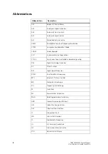
Page 471: ...trol lines 18 1 1 Hardware Flow Control Although the serial transmit and receive lines are dedicated connections on the internal options connector the RTS and CTS lines have to be assigned For hardwar...

Page 472: ...ollowing instructions refer to items in the diagram on page 473 2 Remove the top cover and lid b from the radio to access the options cavity 3 Remove the external options connector bung c if it is fit...

Page 473: ...be installed correctly in the radio s options cavity the internal options connector loom 1 must be looped in the way shown in the diagram on page 473 9 Plug the unattached end of internal options con...

Page 474: ...ap point out of the receive or transmit audio chain DC coupled 3 AGND analogue ground 4 AUX_MIC_AUD Auxiliary microphone input with electret microphone biasing provided Dynamic microphones are not sup...

Page 475: ...50v X7r 10 C18 018 14100 00 Cap 0603 1n 50v X7r 10 LK1 036 14100 10 RES 0805 1k 1 1 8W LK3 036 14100 10 RES 0805 1k 1 1 8W R1 038 15100 10 RES 0603 10k 1 1 10W R2 038 15100 10 RES 0603 10k 1 1 10W R3...

Page 476: ...476 TMAA01 02 RS 232 Board TM8100 TM8200 Service Manual Tait Electronics Limited June 2006 18 4 2 RS 232 Board Layout top side IPN 220 01740 01...

Page 477: ...TM8100 TM8200 Service Manual TMAA01 02 RS 232 Board 477 Tait Electronics Limited June 2006 18 4 3 RS 232 Board Layout bottom side IPN 220 01740 01...

Page 478: ...478 TMAA01 02 RS 232 Board TM8100 TM8200 Service Manual Tait Electronics Limited June 2006 18 4 4 RS 232 Board Circuit Diagram...

Page 479: ...ortant This equipment contains devices which are susceptible to damage from static discharges Refer to ESD Precautions on page 108 for more information The options extender board has various link opti...

Page 480: ...mum current for the 5V supply line is 400mA 19 1 2 RX_BEEP_IN Line If the RX_BEEP_IN line is required on the external options connector it must replace one of the following lines IOP_RSSI AUD_TAP_IN A...

Page 481: ...On the inside of the radio lid place the foam seal d over the external options connector cavity e 5 With the top side of the options extender board f facing the radio lid guide the external options c...

Page 482: ...9 2 8 Plug the unattached end of internal options connector loom 1 into the internal options connector on the radio main PCB 9 Refit the radio lid and top cover to the radio and screw the external opt...

Page 483: ...e TMAA30 01 Table 19 3 Internal options connector pins and signals Pin Connector Signal Description 1 13V8_SW switched 13V8 supply from the radio 2 AUD_TAP_OUT Programmable tap point out of the receiv...

Page 484: ...e RSSI output 15 IOP_GPIO13 programmable function and direction 14 IOP_GPIO2c programmable function and direction 13 IOP_GPIO3c programmable function and direction 10 IOP_GPIO4c programmable function...

Page 485: ...iode BAV99w Dual Ss D7 001 10099 01 Diode BAV99w Dual Ss D8 001 10099 01 Diode BAV99w Dual Ss IC1 002 10020 20 IC SMD ADM202 Rs 232 Con S0 16 IC2 002 10267 40 IC LM2674 S08 Swtch Volt Regul L1 057 101...

Page 486: ...C33 C4 1B1 C34 C4 1B1 C35 C4 1B1 C36 C4 1A1 C4 D4 1G2 C5 D4 1G4 C6 E4 1G7 C7 F3 1G7 C8 E3 1G8 C9 F3 1G6 D1 G3 1G7 D2 B2 1A2 D3 C2 1D2 D4 C2 1C3 D5 B2 1C2 D6 C2 1C3 1B3 D7 C2 1B3 D8 C2 1B2 IC1 D4 1F3 I...

Page 487: ...ervice Manual TMAA01 05 Options Extender Board 487 Tait Electronics Limited June 2006 19 4 3 Options Extender Board Layout top side 19 4 4 Options Extender Board Layout bottom side IPN 220 65203 00 IP...

Page 488: ...488 TMAA01 05 Options Extender Board TM8100 TM8200 Service Manual Tait Electronics Limited June 2006 19 4 5 Options Extender Board Circuit Diagram...

Page 489: ...DTMF microphone is not suitable for use with PTT signalling An example of PTT signalling is leading ANI 20 1 Installation Installing the Microphone Important The DTMF microphone grommet must be insta...

Page 490: ...n 3kHz for wide bandwidth radios and 1 5kHz for narrow bandwidth radios 20 3 Radio Programming The following table shows the settings required for CH_GPIO1 in the Programmable I O form of the programm...

Page 491: ...e connector and shows the interface between the DTMF microphone and the radio Table 20 2 DTMF microphone connector pins and signals Pin Signal Colour Description 1 not connected 2 13V8_SW red power su...

Page 492: ...ption The microphone has a standard 12 key telephone keypad When one of the keypad keys is pressed a DTMF tone specific to that key is generated on the MIC_AUD line pin 5 For the duration of the tone...

Page 493: ...ol head 21 1 Installation Important This equipment contains devices which are susceptible to damage from static discharges Refer to ESD Precautions on page 108 for more information Disassembling the R...

Page 494: ...ve wire to AGND 1 Note The positive wire on the microphone capsule is identified by a red stripe 6 On the control head PCB remove R11 1 and solder P2 1 and P3 1 in the positions shown 7 Plug S2 1 and...

Page 495: ...rom the control head shift register 3 OE enables the output of the shift register of the audio switch 4 CH_SPI_CLK SPI clock signal to clock microphone select data into concealed and dynamic microphon...

Page 496: ...23 Q2 000 10085 71 Xstr SMD BC857BW PNP SOT323 Q3 000 10084 62 Xstr BC846S Dual SOT363 NPN Q4 001 10099 01 Diode BAV99w Dual Ss R1 038 14220 00 Res 0603 2k2 1 16w 5 R2 038 14680 00 Res 0603 6k8 1 16w...

Page 497: ...8100 TM8200 Service Manual TMAA02 06 Support Kit for Concealed Dynamic Microphones 497 Tait Electronics Limited June 2006 21 4 2 Concealed and Dynamic Microphone Support Board top side IPN 220 01712 0...

Page 498: ...TMAA02 06 Support Kit for Concealed Dynamic Microphones TM8100 TM8200 Service Manual Tait Electronics Limited June 2006 21 4 3 Concealed and Dynamic Microphone Support Board bottom side IPN 220 01712...

Page 499: ...TM8100 TM8200 Service Manual TMAA02 06 Support Kit for Concealed Dynamic Microphones 499 Tait Electronics Limited June 2006 21 4 4 Concealed and Dynamic Microphone Board Circuit Diagram...

Page 500: ...500 TMAA02 06 Support Kit for Concealed Dynamic Microphones TM8100 TM8200 Service Manual Tait Electronics Limited June 2006...
Page 501: ...head seal is not damaged Damage to this seal reduces environmental protection 1 On the underside of the radio insert a 5mm 3 16 inch flat bladed screwdriver between the control head and the control he...

Page 502: ...COV MIC pad f Note The positive wire on the micro phone capsule is identified by a red stripe 5 Re install adaptor flange onto the control head 6 Plug the control head loom onto the control head conne...

Page 503: ...is connected to the microphone clip and open when the microphone is removed from the microphone clip The function of the hookswitch is determined by the way the radio is programmed 23 1 Operation Dia...

Page 504: ...e radio is powered on so that if the microphone is plugged in after the radio has been powered on it will not recognize the keypad microphone Also if the keypad microphone is plugged in on power up bu...

Page 505: ...can program the radio to dial labels or channels from the default display Refer to the online help of the programming application for more information about these programming options MPT1327 Trunked F...

Page 506: ...506 TMAA02 08 Keypad Microphone TM8100 TM8200 Service Manual Tait Electronics Limited June 2006...

Page 507: ...TMAA03 02 security bracket are illustrated in Figure 24 1 Figure 24 1 Parts of the TMAA03 02 security bracket Description Quantity B security bracket cradle base 1 E short mounting rails for TM8100 2...

Page 508: ...wise there is a risk that the whole assembly of the radio and secu rity bracket may become loose over time or as a result of serious impact Note Because some model control heads are taller than others...

Page 509: ...Bracket Remove the radio from the security bracket as follows 1 Open the slide locks by inserting the slide lock key into the keyhole Rotate the key 90 it will slip into a detent and pull The pull wi...

Page 510: ...be installed at different times Part Part Number Quantity Security Crdl Key TM8 slide lock key 319 60004 XX1 1 Contact Technical Support for the exact IPN 2 Security Crdl Mtg Short TM8 short mounting...

Page 511: ...ot compatible with TMAA03 03 TMAC34 0T or TMAC34 1T control head interfaces 25 1 Installation Warning Mount the remote U bracket with the remote control head assembly and the U bracket with the radio...

Page 512: ...remote U bracket 5 Mount the U bracket in the required position and install the radio body in the U bracket 6 Route the remote cable e between the remote control head assembly and the radio body 25 1...

Page 513: ...the radio body The control head is now separate from the radio body 25 1 4 Installing the Torso Interface The torso interface must be installed onto the radio body in place of the control head 1 Screw...

Page 514: ...ote U bracket in the chosen mounting position using the self drilling screws provided Use all four screws provided 25 1 6 Installing the Control Head Interface With the control head separated from the...

Page 515: ...ortant When mounting the U bracket check whether the mounting surface needs to be reinforced Important Install the U bracket using at least four screws 1 If the U bracket is being mounted over a curve...

Page 516: ...ote Cable Grommets Install both the remote cable grommets using the following procedure Important The remote cable grommets must be installed whenever the remote cable is plugged into the RJ45 sockets...

Page 517: ...d June 2006 25 2 Circuit Description Figure 25 3 shows a block diagram of the remote control head installation The control heads contain circuit boards with RS 485 driver components and an audio ampli...

Page 518: ...le from the RJ45 connector 2 Release the clips of the PCB bracket E and remove the control head board B 3 Disconnect the torso interface loom C 4 Unscrew the four PT type screws D and remove the PCB b...

Page 519: ...rried out in reverse order of disassembly 1 Remove the remote cable from the RJ45 connector 2 Unscrew the seven PT type screws B and remove the PCB C 3 Remove the control head interface loom not illus...

Page 520: ...TH J101 240 10000 11 Conn SMD 18w Skt M Match Q101 000 10084 73 Xstr BC847BPNNPN PNP SOT363 R101 038 10000 00 Res 0603 Zero 0hm 1 16w 5 R102 036 03100 10 Res 2512 100R 5 1W R103 036 03100 10 Res 2512...

Page 521: ...C4 D103 G4 1E2 D104 J4 1E3 D105 F4 1D4 1D3 D106 D4 1B2 D107 M4 1D7 E101 F3 1B2 E102 F4 1B3 E103 G1 1C3 E104 G1 1C3 E105 K3 1D1 E106 D3 1D1 E107 E4 1D2 E108 E4 1C2 E109 K1 1D5 F101 F3 1D2 J100 E4 1C1 J...

Page 522: ...522 Installing a Remote Kit TM8100 TM8200 Service Manual Tait Electronics Limited June 2006 Board Layout IPN 220 02122 02...

Page 523: ...TM8100 TM8200 Service Manual Installing a Remote Kit 523 Tait Electronics Limited June 2006 Circuit Diagram...

Page 524: ...40 10000 11 Conn SMD 18w Skt M Match J3 240 00016 00 Conn RJ45 Shld 8P8C LP RA TH Q1 000 10561 60 XSTR BCX56 16 AF NPN SOT89 R1 038 13100 10 Res 0603 100R 1 10w 1 R3 038 15100 10 Res 0603 10k 1 10w 1...

Page 525: ...TM8100 TM8200 Service Manual Installing a Remote Kit 525 Tait Electronics Limited June 2006 Board Layout IPN 220 02123 01...

Page 526: ...526 Installing a Remote Kit TM8100 TM8200 Service Manual Tait Electronics Limited June 2006 Circuit Diagram...

Page 527: ...cket with the radio body securely These units must not break loose in the event of a collision Unse cured radio units are dangerous to the vehicle occupants Caution Observe the installation warnings a...

Page 528: ...the remote U bracket 5 Mount the U bracket in the required position and install the radio body in the U bracket 6 Route the remote cable e between the remote control head assembly and the radio body...

Page 529: ...trol head loom from the radio body The control head is now separate from the radio body 26 1 4 Installing the Torso Interface The torso interface must be installed onto the radio body in place of the...

Page 530: ...stalling the Control Head Interface With the control head separated from the radio body the control head interface c must be installed on the rear of the control head 1 Undo the two Torx T 20 screws o...

Page 531: ...ition using the two thumb screws provided 26 1 7 Mounting the U Bracket and Installing the Radio Body Mounting the U Bracket Install the U bracket on any sufficiently flat surface using self drilling...

Page 532: ...in the holes 2 Plug one end of the remote cable into the control head interface 3 Run the remote cable to the torso interface and plug it into the RJ45 connector without a bung Installing the Remote...

Page 533: ...onics Limited June 2006 26 2 Circuit Description Figure 26 3 shows a block diagram of the remote control head installation Both control heads contain a circuit board with audio amplifiers and RS 485 d...

Page 534: ...er of disassembly 1 Release the clip of the PCB bracket E and remove the control head board B 2 Disconnect the torso interface loom C 3 Unscrew the four PT type screws D and remove the PCB bracket E F...

Page 535: ...nector loom Re assembly is carried out in reverse order of disassembly 1 Unscrew the seven PT type screws B and remove the PCB C 2 Remove the control head interface loom not illustrated Figure 26 5 Pa...

Page 536: ...001 10000 99 Diode SMD BAV99 D Sw SOT23 D110 001 10084 91 Diode SMD BZX84C9V1 Zen SOT23 D201 001 10000 99 Diode SMD BAV99 D Sw SOT23 D211 001 10000 99 Diode SMD BAV99 D Sw SOT23 D300 001 10000 99 Dio...

Page 537: ...RJ45 Shortbody Plg 360 02022 00 Grommet Mic TMA Grid Reference List C1 D1 D7 C100 J3 E3 C101 L4 E3 C102 J4 E3 C103 J4 E3 C110 L4 F4 C300 M5 G2 C301 N5 G3 C310 M2 G4 C311 N2 G4 C312 M2 G5 C320 P4 D8 C...

Page 538: ...538 Installing an Enhanced Remote Kit TM8100 TM8200 Service Manual Tait Electronics Limited June 2006 Board Layout IPN 220 01721 04...

Page 539: ...TM8100 TM8200 Service Manual Installing an Enhanced Remote Kit 539 Tait Electronics Limited June 2006 Circuit Diagram...

Page 540: ...03 0R R21 038 10000 00 RES 0603 0R R30 038 13390 10 RES 0603 390R 1 1 10W R31 038 13390 10 RES 0603 390R 1 1 10W R40 036 00000 01 RES 1206 0R 5 0 25W R103 038 12100 10 RES 0603 10R 1 1 10W R104 038 15...

Page 541: ...TM8100 TM8200 Service Manual Installing an Enhanced Remote Kit 541 Tait Electronics Limited June 2006 Board Layout IPN 220 01720 05...

Page 542: ...542 Installing an Enhanced Remote Kit TM8100 TM8200 Service Manual Tait Electronics Limited June 2006 Circuit Diagram...

Page 543: ...smit tail is required settings in the following forms must be configured in both radios PTT form TM8100 radios only refer to Table 27 4 Basic Settings form Subaudible Signalling tab TM8200 radios and...

Page 544: ...able 27 2 Crossband settings in the Programmable I O form Digital tab Pin Direction Label Action Active Debounce Signal State Mirrored To AUX_GPI1 Input PTT_INS External PTT 1 Low 10 None None AUX_GPI...

Page 545: ...olerance of 200Hz on a 12 5kHz narrow bandwidth channel 27 4 Interface Specification The following table and diagram summarizes the signals used for the crossband linking cable on the radios auxiliary...

Page 546: ...100 00 Cap 0603 100n 16v x7r 10 C10 018 16100 00 Cap 0603 100n 16v x7r 10 J1 240 00031 00 Plg 15w Drng UL CSA Pnl Mtg R1 038 13560 10 RES 0603 560R 1 1 10W R6 038 13560 10 RES 0603 560R 1 1 10W 205 00...

Page 547: ...TM8100 TM8200 Service Manual TMAA04 04 Crossband Linking Cable 547 Tait Electronics Limited June 2006 27 5 2 Crossband Linking Board Layouts IPN 220 02127 01...

Page 548: ...548 TMAA04 04 Crossband Linking Cable TM8100 TM8200 Service Manual Tait Electronics Limited June 2006 27 5 3 Crossband Linking Board Circuit Diagram...

Page 549: ...urns on or returns to the state that it was in when the vehicle ignition was turned off Important The radio does not meet the IP54 protection standard once the bung for the auxiliary connector is remo...

Page 550: ...550 TMAA04 05 Ignition Sense Kit TM8100 TM8200 Service Manual Tait Electronics Limited June 2006...

Page 551: ...microphone and release the PTT key when you have finished talking Note The monitor key can be locked in the on position To do this hold the monitor key down and slide the monitor key towards you The m...

Page 552: ...imum by rotating R5 counterclockwise 29 4 Interface Specification The following table and diagram summarizes the signals used for the desktop microphone on the radio s microphone connector and shows t...

Page 553: ...le and contains a pre amplifier Q1 to boost the microphone level to that required by the radio Power for the pre amplifier is provided by the electret microphone bias circuit within the radio R5 is us...

Page 554: ...554 TMAA10 01 Desktop Microphone TM8100 TM8200 Service Manual Tait Electronics Limited June 2006...

Page 555: ...om any connected remote speaker and from the handset earpiece Using private handset mode the radios internal and external speakers are muted and the call can only be heard from the handset earpiece 30...

Page 556: ...stalled when ever the handset to radio cord is plugged into the microphone socket When installed the grommet has two functions to prevent damage to the microphone socket when there is movement of the...

Page 557: ...mmable I O form of the radio s programming application Refer to the online help of the programming application for more information Note If private handset mode is programmed then no audio will be hea...

Page 558: ...n the handset and the radio Table 30 5 Handset microphone connector pins and signals Pin Signal HandsetPCB Connector Colour Description 1 RX_AUD 8 brown receive audio to handset 2 not connected 3 not...

Page 559: ...re included with each kit along with four mounting screws and washers 31 1 Installation Remote Speaker Mounting 1 Choose a mounting position for the remote speaker where it will not interfere with the...

Page 560: ...the positive wire and receptacle into the position nearest to the red wire and the negative wire and receptacle into the position nearest to the black wire 2 TMAA10 06 remote speaker 40W 50W radios Fo...

Page 561: ...nds Free Kit Your radio may able to detect the sound of your voice so that you can make calls without using the PTT key Voice operated transmit VOX is turned on and off either by using a function key...

Page 562: ...e taken to avoid routing any cables near vehi cle pedal controls steering column and other moving parts Installing the Remote Microphone 1 Choose one of the three mounting options provided for the rem...

Page 563: ...ion When Mic On Hook field is selected in the PTT tab of the PTT form Remote PTT Settings in the Programmable I O Form The following table shows the settings required in the Programmable I O form of t...

Page 564: ...hands free kits on the radio s auxiliary connector and shows the interface between the kits and the radio Table 32 3 VOX settings in the PTT form External PTT 2 or VOX tab Field Setting EPTT2 or VOX I...

Page 565: ...voltage for the regulator is provided by AUX_GPIO4 line The remote microphone signal is fed via AUX_MIC_AUD and an input selector to the radio s internal microphone amplifier The microphone input sel...

Page 566: ...NPN SOT323 Q2 000 10085 71 Xstr SMD BC857BW PNP SOT323 Q3 000 10084 71 Xstr BC847BW NPN SOT323 Q4 000 10084 71 Xstr BC847BW NPN SOT323 R1 038 14220 00 Res 0603 2k2 1 16w 5 R3 038 14390 10 Res 0603 3k9...

Page 567: ...TM8100 TM8200 Service Manual TMAA10 04 Remote PTT Kit and TMAA10 05 Hands Free Kit 567 Tait Electronics Limited June 2006 32 7 2 Pre Amplifier Board Layout IPN 220 01711 01 IPN 220 01711 01...

Page 568: ...568 TMAA10 04 Remote PTT Kit and TMAA10 05 Hands Free Kit TM8100 TM8200 Service Manual Tait Electronics Limited June 2006 32 7 3 Pre Amplifier Board Circuit Diagram...

Page 569: ...press the TRANSMIT key PTT to transmit Speak clearly into the microphone and release the TRANSMIT key when you have finished talking Note The MONITOR key can be locked in the on position To do this h...

Page 570: ...4 Radio Programming The desktop microphone has an internal pre amplifier Therefore the dynamic microphone support in the UI Preferences form of the radio s programming application should not be enabl...

Page 571: ...ns test set The diagram below shows the front panel of the test unit 34 1 Test Equipment Setup The diagram on the following page shows how the test unit is connected to the radio the test PC and the R...

Page 572: ...onnector BNC computer connector RJ12 serial port DB9 speaker connector banana plugs AC input BNC audio monitor out BNC AUDIO IN HI BNC AUDIO OUT BNC RF in out N type power connector TMAA23 02 cable 50...

Page 573: ...tch is used to switch between Mod Audio Audio Tap In Mic Audio and Off no audio signal With the Tait Orca portables this switch can be used for setting up dual point modulation by applying modulation...

Page 574: ...isconnect the radio s internal speaker on mobiles If the switch is set to Speaker or Load this simulates an external speaker being connected in parallel to the radio s internal speaker With all settin...

Page 575: ...032 31820 01 Res M F Pwr 17x5 8e2 5 2 5w R2 032 31820 01 Res M F Pwr 17x5 8e2 5 2 5w R3 030 55120 20 Res Flm 4x1 6 12k 5 0 4w R4 030 53560 20 Res Flm 4x1 6 560e 5 0 4w R5 030 54270 20 Res Flm 4x1 6 2k...

Page 576: ...y Refer to the parts list for actual values used SPEAKER 4 SPKR 8 2 SHOULD BE DPTT IPN 032 31820 01 IPN 250 00010 19 not part of PCB not fitted not fitted not fitted Portable Mobile Mobile Portable Po...

Page 577: ...REVERSE COMPILE OR REVERSE ASSEMBLE ANY SOFTWARE OR FIRMWARE IN WHOLE OR PART Important Notice THE SOFTWARE OR FIRMWARE MAY CONTAIN OPEN SOURCE SOFTWARE COMPONENTS OPEN SOURCE COMPONENTS OPEN SOURCE...

Page 578: ...OLE AND TOTAL LIABILITY FOR ANY SUCH CLAIM SHALL BE LIMITED AT THE OPTION OF TAIT TO THE REPAIR OR REPLACEMENT OF THE SOFTWARE OR FIRMWARE OR THE REFUND OF THE PURCHASE PRICE OF THE SOFTWARE OR FIRMWA...

Reviews: