B IT PATTERN~
BIT C E L L
P+
)
0
1
0
I
I
I
I
C
)D
C
I
)
I
I
I
I
I
)
)
)
)
)
0
I
I
I
I
1
I
I
)
I
)
MAGNETIZATION
WRITE DATA
D / C
I
I
I
I
D I C
I
c I
c
I
I
D
C
I
I I
I
I
I
I
I
MAGNETIC ELEMENTS
N
S S N N S S
S S N N S S
I
I
)
I
I
I
I
)
)
I
I
I
•
I
)
I
s
I
)
I
I
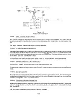
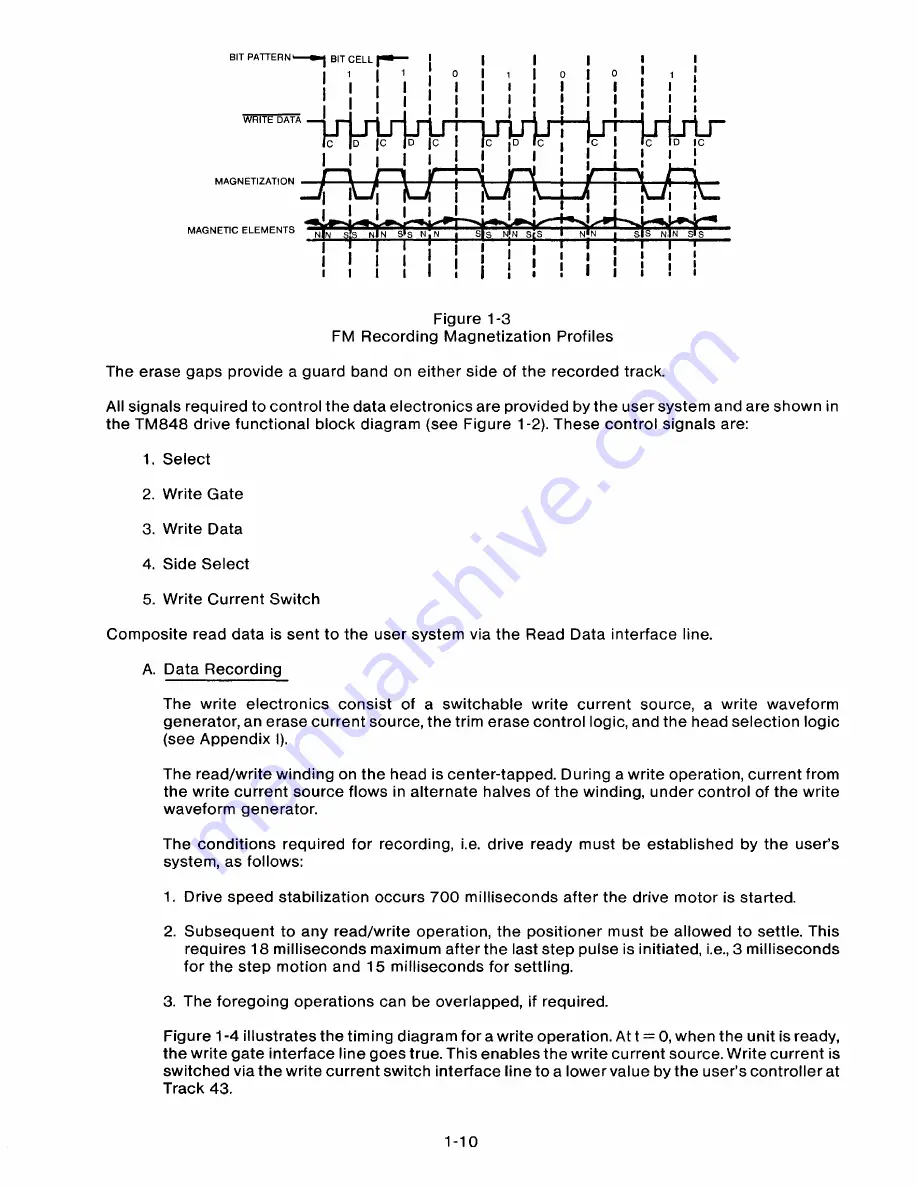
Figure 1-3
FM Recording Magnetization Profiles
The erase gaps provide a guard band on either side of the recorded track.
All signals required to control the data electronics are provided by the user system and are shown in
the TM848 drive functional block diagram (see Figure 1-2). These control signals are:
1. Select
2. Write Gate
3. Write Data
4. Side Select
5. Write Current Switch
Composite read data is sent to the user system via the Read Data interface line.
A. Data Recording
T he write e l e c t ronics c o n s ist o f a s w i t c h a ble w r it e c u r r ent s o u r ce, a w r it e w a v e f o rm
generator, an erase current source, the trim erase control logic, and the head selection logic
(see Appendix I).
The read/write winding on the head is center-tapped. During a write operation, current from
the write current source flows in alternate halves of the winding, under control of the write
waveform generator.
The conditions required for re cording, i.e. drive ready must be e s t a blished by th e u s e r's
system, as follows:
1. Drive speed stabilization occurs 700 milliseconds after the drive motor is started.
2. Subsequent to any read/write operation, the positioner must be allowed to settle. This
requires 18 milliseconds maximum after the last step pulse is initiated, i.e., 3 milliseconds
for the step motion and 15 milliseconds for settling.
3. The foregoing operations can be overlapped, if required.
Figure 1-4 illustrates the timing diagram for a write operation. At t = 0, when the unit is ready,
the write gate interface line goes true. This enables the write current source. Write current is
switched via the write current switch interface line to a lower value by the user's controller at
Track 43.
1-10
Summary of Contents for TM848-1
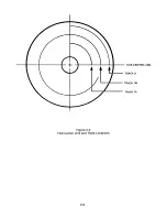
Page 32: ...HUB CENTER LINE TRACK 0 TRACK 38 TRACK 76 Figure 2 2 Hub Center Line and Track Locations 2 3 ...
Page 81: ...APPENDIX I PRINTED CIRCUIT BOARD S CHEM A T ICS AND ASSEM B LY DRAW IN G S ...
Page 88: ...APPENDIX II RECOM M E N D E D SPARE PARTS LIST ...
Page 90: ...Pi N 1 79031 001 1 082 ...


