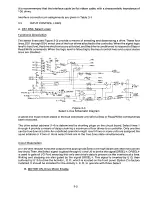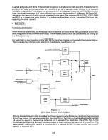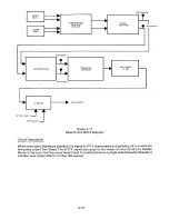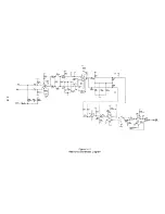
TEST POINT 2
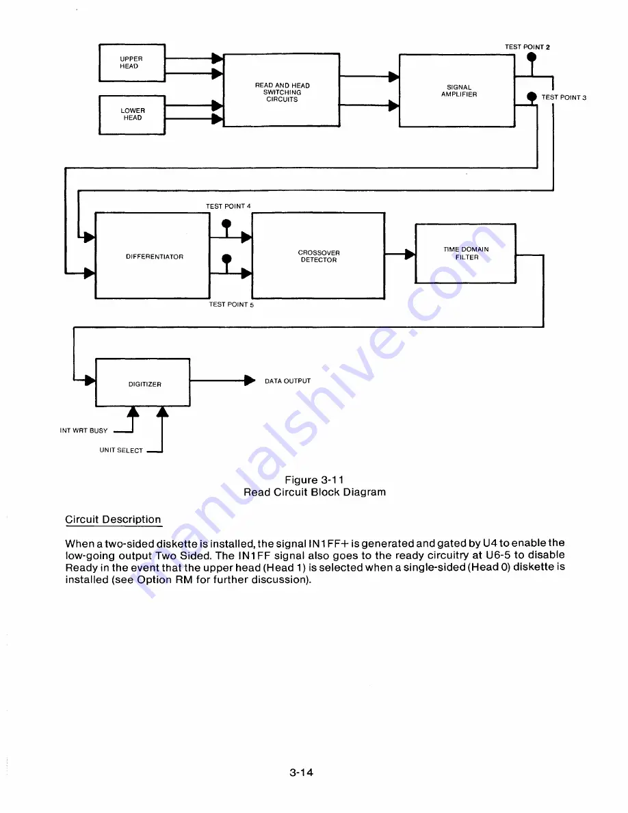
UPPER
HEAD
READ AND HEAD
SWITCHING
CIRCUITS
SIGNAL
AMPLIFIER
TEST POINT 3
LOWER
HEAD
TEST POINT 4
TIME DOMAIN
DIFFERENTIATOR
CROSSOVER
DETECTOR
FILTER
TEST POINT S
DATA OUTPUT
DIGITIZER
INT WRT BUSY
UNIT SELECT
Figure 3-11
Read Circuit Block Diagram
Circuit Description
When a two-sided diskette is installed, the signal IN1FF+ is generated and gated by U4 to enable the
low-going output Two Sided. The IN1FF signal also goes to the ready circuitry at U6-5 to disable
Ready in the event that the upper head (H ead 1) is selected when a single-sided (Head 0) diskette is
installed (see Option RM for further discussion).
3-1 4
Summary of Contents for TM848-1
Page 32: ...HUB CENTER LINE TRACK 0 TRACK 38 TRACK 76 Figure 2 2 Hub Center Line and Track Locations 2 3 ...
Page 81: ...APPENDIX I PRINTED CIRCUIT BOARD S CHEM A T ICS AND ASSEM B LY DRAW IN G S ...
Page 88: ...APPENDIX II RECOM M E N D E D SPARE PARTS LIST ...
Page 90: ...Pi N 1 79031 001 1 082 ...

