background image

APPENDIX  II

REC O M M

E N D E D S P A R E  P A R T S  LIST

Summary of Contents for TM848-1

Page 1: ...VICE MANUAL TM848 1 ANDTM848 2 DISK DRIVES 48 TRACKSPERINCH mn d u n coR poRATIDN 20320 PRAIRIE STREET CHATSWORTH CA 91311 TELEPHONE NO 213 993 6644 TWX NO 91 0 494 1 721 TEL EX NO 194794 COPYRIGHT 1982 TANDON CORPORATION ...

Page 2: ...nt is the property of Tandon Corporation It may not be duplicated in full or part by any person without prior written approval The material in this document is provided for informational purposes and is subject to change by Tandon Corporation ...

Page 3: ... The Drive Organization of The Drive Components of The Drive Index Pulse Drive Status Logic Spindle Drive System Positioner Control Data Electronics Interface Electronics Interface Connector Pin Assignments P13 Power Connector Pin Assignments Terminated Lines Input Line Terminations From Removable Resistor Pack Drive Select Program Shunt DS and HL Power Save Options User Selectable Options Drive S...

Page 4: ...dex To Data Burst Checks Index Sensor Adjustment Index Pulse Width Check Track 00 Sensor Check and Adjustment Amplitude Check Azimuth Check Load Arm Adjustment 2 1 2 1 2 1 2 2 2 4 2 5 2 6 2 6 2 7 2 8 2 8 2 9 2 10 2 10 Introduction Physical Description of The Circuit Board Interface Electronics Specifications Input Control Lines O utput Control Lines 3 1 3 1 3 1 3 2 3 7 3 3 1 3 2 3 3 3 4 SECTION IV...

Page 5: ...ensor Assembly Diskette Ejector Assembly Load Resistor Assembly Stepper Band Stepper Motor Assembly Head Carriage Assembly 5 8 5 9 5 10 5 1 1 5 1 2 5 1 3 5 1 4 5 1 5 5 I 6 5 1 7 5 I 8 APPENDIX I PRINTED CIRCUIT BOARD SCHEM ATICS AND ASSEMBLY 5 9 5 1 0 5 10 5 1 1 5 1 2 5 12 5 1 4 5 1 5 5 1 6 5 18 5 1 9 DRAWINGS 11 1 APPENDIX II RECOMM E N D E D SPARE PARTS LIST ...

Page 6: ...ng Pulse Width Track 00 Sensor Optimum Head Azimuth Alignment Head Azimuth Alignment Acceptable Lower Limits Head Azimuth Alignment Acceptable Upper Limits Load Arm Adjustment Front View Printed Circuit Board Interface Configuration Select Lines Schematic Diagram Write Data Circuit Block Diagram Trim Erase Diagram Side Select Schematic Diagram Index Schematic Diagram Waveform at Test Point 7 Soft ...

Page 7: ...mbly Key Parts Bottom View Diskette Ejector Assembly Key Parts Load Resistor Assembly and Key Parts Stepper Band Key Parts Stepper Band Additional Key Parts Stepper Motor Assembly Key Parts Head Carriage Assembly Key Parts TABLES 5 15 5 1 6 5 1 7 5 1 8 5 1 9 5 20 5 1 9 5 20 5 21 5 22 5 23 Table Number Page Number Title of Table Mechanical and Electrical Specifications Power Requirements Interface ...

Page 8: ...d assembly is a glass bonded manganese zinc ceramic structure It has a life in excess of 20 000 hours For diskette loading operator access is provide via a slot located on the front of the drive The electronic components of the drive are mounted on a circuit board assembly located in the chassis Power and interface signals are routed through connectors that plug into the back of the drive 1 3 FU N...

Page 9: ...installed This output signal is present at the interface 3 The Write Protect sensor disables the drive s write electronics whenever a write enable tab is removed from the diskette see Section 1 12 1 4 DISKET T ES The drive uses a standard eight inch diskette Diskettes are available with a single index hole or with index and sector holes They also are available double or single sided Single index h...

Page 10: ... Wear Guarantee Number of Tracks Track To Track Access Time Head Settling Time Average Access Time including head settling time Motor Start Time Disk Rotational Speed Instantaneous Speed Variation Flux Changes Per Inch Inside Track Transfer Rates Linformatted Recording Capacity 1 in 10 bits 1 in 10 bits 1 in I 0 seeks 10 000 power on hours 30 minutes IBM Format Recording Capacity 15 000 media hour...

Page 11: ...cal Total 0 92 Amps typical 3 24 Volts During motor start interval a Configured for stepper motor enabled during motor start 2 5 Amps typical surge 2 5 2 0 1 5 1 0 0 5 100 200 300 400 600 500 TIME MILLISECONDS b Configured for stepper motor disabled until motor comes up to speed 2 1 Amps typical surge 2 5 2 0 STEPPER MOTOR ENABLED 1 5 1 0 0 5 200 300 400 500 600 100 TIME MILLISECONDSI 1 4 ...

Page 12: ...drive passes all the checks listed above it is operational If not review Section II INTERFACE CONNECTIONS 1 9 Signal connections for the drive are made via a user supplied 50 pin flat ribbon connector 3M Scotchflex 3415 This connector mates directly with the circuit board connector at the rear of the drive The D C power connector is a six pin connector Amp Mate N Lok Part Number 1 480270 0 which m...

Page 13: ...C over The design of an enclosure should incorporate a means to prevent contamination from loose items e g dust lint and paper since the drive does not have a dust cover 1 10 3 Cool ing System Requirements Heat dissipation from a single drive is normally 30 watts 102 Btu Hr under high line conditions When the drive is mounted so that the components have access to the free flow of air normal convec...

Page 14: ... on the board for defeating the write protect sensor 1 13 OPERA T ION OF THE DRIVE The drive consists of the mechanical and electrical components necessary to record and to read digital data on a diskette User provided D C power at 24 volts and 5 volts is required for operation of the drive 1 14 ORGAN I ZATION OF THE DRIVE All electrical subassemblies in the drive are constructed with leads that t...

Page 15: ...00 Sensor Two Sided Ready and Disk Change A Write Protect A write protect signal is provided to the user s system via the write protect interface line The write protect circuitry consists of a write protect sensor and circuitry that routes the signal that is produced When a write protected diskette is inserted in the drive the sensor is activated and the logic disables the write electronics and su...

Page 16: ...ND STEPPER BAND ASSEMBLY WR ITE PROTECT DETECTOR DRIVE SELECT SPINDLE MOTOR CONTROL MOTOR CONTROL D C DRIVE MOTOR WRITE GATE WRITE DATA WRITE LOGIC CURRENT SWITCH READ LOGIC READ DATA DIRECTION STEPPER MOTOR CONTROL STEP Figure 1 2 TM848 Disk Drive Functional Block Diagram 1 15 4 Posi t ioner Control The head positioning system uses a bipolar driven motor drive which changes one phase for each tra...

Page 17: ...rol logic and the head selection logic see Appendix I The read write winding on the head is center tapped During a write operation current from the write current source flows in alternate halves of the winding under control of the write waveform generator The conditions required for recording i e drive ready must be established by the user s system as follows 1 Drive speed stabilization occurs 700...

Page 18: ... NOTES 1 T 0 700 MILLISECONDS AFTER DRIVE MOTOR STARTS OR 20 MILLISECONDS AFTER LAST STEP PULSE WHICHEVER IS THE LATEST TIME 3 10 MA PEAK TO PEAK TRACK 0 TO TRACK 42 7 5 MA PEAK TO PEAK TRACK 43 TO TRACK 77 2 UNS YCHRONIZED 4 2 USEC MINIMUM 4 USEC MAXIMUM Figure 1 4 Write Operation Timing Diagram The duration of a write operation is from the true going edge of write gate to the false going edge of...

Page 19: ...ds after a step command or 100 microseconds after termination of write busy whichever is the latest time The zero crossover detector and digitizer circuitry generate a 200 nanosecond read data pulse corresponding to each peak of the read signal The composite read data signal is sent to the user system via the read data interface line 1 16 I NTER FACE ELECTRONICS All interface signals are TTL compa...

Page 20: ...option Side Select Model TM848 2 only Activity Indicator option Head Load Index Ready Motor Off Control 4 Drive Select 1 Side Select Option TM848 2 only Drive Select 2 Side Select Option TM848 2 only Drive Select 3 Side Select Option TM848 2 only Drive Select 4 Side Select Option TM848 2 only Direction Select Side Select Option TM848 2 only Step Write Data Write Gate Track 00 Write Protect Read Da...

Page 21: ... controller When the signal logic level is true low the drive electronics are activated and the drive is conditioned to respond to Step or to Read Write commands When the signal logic level is false high the input control lines and the output status lines are disabled The drive select address is determined by a movable shorting plug installed on the circuit board Select lines one through four prov...

Page 22: ... 4b 0 oo DS4 0 0 RM MC3 TP5 00 00 Q 0 IZ 0 TP4 PT6 MC200 MC1 0 0 C MC4 0 S2 0 O S1 D o 32 NP Oo Y ALTERNATE TEST POINT INDEX TRIGGERING RPI O Qas2 R133 DSI WP TP11 0 0 T P12 Ml g P13 50 TP 7 0 0 TPS o ODL OTPS OTP10 00 3 M2 IL P6 P14 P2 P3 P10 P1 P I P12 Figure 1 6 Circuit Board Assembly ...

Page 23: ...INIMUM DIRECTION SELECT 1 USEC MINIMUM 1 USEC MINIMUM STEP 1 USEC M I Nl MUM 3 MILLISECONDS MINIMUM SIDE SELECT 100 NSEC MINIMUM WRITE GATE 4 USEC MAXIMUM WRITE DATA 18 MSEC MINIMUM VALI READ DATA 100 USEC MAXIMUM 550 USEC MINIMUM Figure 1 7 General Control and Data Timing Requirements 1 16 ...

Page 24: ...hould be used in conjunction with the following list of options that are available for model numbers TM848 1 and TM848 2 see Table 1 5 TABLE 1 5 OPTIONS AS SH IPPED TRACE OPTION Drive Select Side Select Options using Drive Select In Use Drive Select In Use Head Load Ready Alternate Output Pad Radial Ready Ready Modified Radial Index Index Alternate Output Pad In Use Alternate Output Pad Diskette L...

Page 25: ...e activity L E D when the drive is selected In Use From Drive Select is factory installed 1 19 4 In Us e From Head Load Y This option allows the user to use the head load line to enable the Activity L E D In Use From Head Load is implemented by punching out Option Z between Pins 1 and 16 of U3 A jumper must be installed at location Y 1 19 5 Read y Alternate Output Pad R This low going signal is de...

Page 26: ...rface of a single sided diskete is selected To implement this option connect a jumper at the RM pads 1 19 8 Radial Index Rl This option uses the alternate I O lines for radial index lines This option allows the user to monitor the index of each drive independent of drive select This option cannot be used concurrently with radial ready or with independent motor control Radial Index is implemented b...

Page 27: ... IN USE low The solenoid is unlatched when drive select is pulsed and 5I USE is high To implement this option locate option pads D and DL Install jumpers at these locations 1 19 11 D iskette Lever Lock Latch Option DL This option is used in conjunction with in use alternate output pad To implement this option locate option pads D and DL Install jumpers at these locations see Section 1 1 8 1 19 12 ...

Page 28: ... connector P13 1 19 17 R a dial Head Load Signal Options A B and X By selection of the appropriate combination of the A B or X jumper the user can use either Drive Select or Head Load to activate the Activity L E D and Lever Lock Solenoid option see Figure 1 10 R4 Dsl DSI 2 1 IB 052 2 S Clss 30 Dsa P D SZ 4 L S04 35 ZB DS S 054 C7 4 7VIP L 300 Ul Nl 15 US QZ at STREOI HEAD LOAD SOLELIOID to Ul 2 1...

Page 29: ...e drive motor using drive select When the drive select line goes low true the drive motor comes up to speed in less then 500 milliseconds and becomes ready in less than 700 milliseconds After the drive select line goes false high the motor will run for 20 seconds To implement this option install a jumper at location M3 For correct operation of M3 remove M4 M4 is used to start the drive motor using...

Page 30: ...lecting the upper or lower head and writing a 1F all zeros if FM or a 2F all ones if FM pattern on the disk 3 A Phillips screwdriver 4 A set of Allen wrenches 5 A flat blade screwdriver 6 A blank diskette 7 An alignment diskette D y san P N 360 2A or equivalent 8 Integrated circuit dip clips 14 and 16 pin SPINDLE DRIVE MOTOR CHECKS AND ADJUSTMENTS 2 1 The long term drive motor speed adjustment ens...

Page 31: ...ATE TEST POINT INDEX TRIGGERING NP 00 DS2 Ds1 WP M III TPII O Q O P12 50 TP T OTPS 8 M2 0 TPS OTPIO 0 DL IZ 00 PS P14 P2 P3 PI O PI PI I P 12 Figure 2 1 Circuit Board Assembly F Adjust R133 until a reading of 166 667 milliseconds is achieved from leading edge to leading edge of the index pulses G If the drive motor s speed cannot be adjusted see Section IV Troubleshooting Guide 2 2 CATS EYE ALIGNM...

Page 32: ...HUB CENTER LINE TRACK 0 TRACK 38 TRACK 76 Figure 2 2 Hub Center Line and Track Locations 2 3 ...

Page 33: ...d drives R33 end closest to DS2 negative trigger is an alternate test point for both single and double sided drives B Apply power to the drive Note The Track 38 radius is 2 8207 2 0020 Other track locations are computed based upon 48TPI C Select the drive at the interface D Insert the alignment diskette into the drive E Select Head 00 the lower head F Seek to and observe Track 38 for Cats Eye alig...

Page 34: ...ep H the head carriage must be adjusted HEAD CARRIAGE ADJUSTMENT 2 3 A Turn the two position retaining screws that straddle the nylon adjustment cam located beneath the drive until the cam can be moved see Figure 2 4 POSITION RETAINING SCREWS 2 O OG p op Is 0 0 0 ADJUSTMENT CAM Figure 2 4 Head Module Retaining and Cam Screws B Observe the Cats Eye pattern from the head that is farthest out of alig...

Page 35: ...Differentially Channel A Channel B Single sided drives trigger on right lead of R33 closest to DS2 negative edge double sided drives trigger on Test Point 12 negative edge A plus B B inverted Test Point 2 Test Point 3 50 microseconds per division Time Base E Insert an alignment diskette F Seek to Track 1 G Select Head 00 the lower head H Ensure that the index to data burst occurs at 200 microsecon...

Page 36: ...t on Track 76 L On a double sideddrive check Heads 01 and 00 the upper and lower heads Note If any index measurement does not meet the specification the index sensor must be adjusted see Section 2 4 2 2 4 2 Index S ensor Adjustment A Loosen the index sensor s retaining screw located on the underside of the chassis see Figure 2 6 o o INDEX SENSOR RETAINING SCREW 0 0 6 0 e o J Figure 2 6 Index Senso...

Page 37: ...dex test point see Section 2 Item Number 1 Test Point 1 5 millisecond per division 2 volts per division Negative leading edge of Channel A appropriate test point Time Base Voltage Trigger B Ensure that the negative going pulse width is between 1 0 and 2 3 milliseconds see Figure 2 7 1 8 to 2 3 milliseconds Figure 2 7 Negative Going Pulse Width 2 5 TRACK 0 0 SENSOR CHECK AND ADJUSTMENT The Track 00...

Page 38: ...e oscilloscope attached as above K Seek out to Track 2 and loosen the two retaining screws that hold the Track 00 sensor see Figure 2 8 TRACK 00 SENSOR I P2 PS Pl RETAINING SCREWS 0o Figure 2 8 Track 00 Sensor L Push the sensor toward the back of the drive and slowly push it forward until the signal on the oscilloscope just goes low true M Tighten the retaining screws and repeat Steps E through I ...

Page 39: ...does not improve the amplitude K If replacing the circuit board does not correct the amplitude replace the Head Carriage Assembly 2 7 AZIMUT H CHECK Azimuth is the angle of the heads with respect to the track at the point of the read write gap Azimuth is measured in minutes one minute 1 60 degree A Set up an oscilloscope as follows Channel A Test Point 2 100 mV per division Channel B Test Point 3 ...

Page 40: ...rved the Cats Eye alignment should be checked prior to any corrective action 3 Figure 2 10 Head Azimuth of Acceptable Lower Limits F Figure 2 11 depicts an alignment of exactly plus 9 12 or 18 minutes depending upon the manufacturer of the diskette used Bursts 3 and 4 are of equal amplitude This is the upper limit of allowable azimuth error If this signal is observed the Cats Eye alignment should ...

Page 41: ...he diskette lever to load the disk and seek to Track 00 There should be a space of 015 inch minimum between the head load arm and the load plate C Seek to Track 76 and ensure that a space of 015 inch minimum remains between the head load arm and the load arm D Adjust the screw located behind the head load cam until the foam just touches the platen E Insert a work diskette and ensure that there is ...

Page 42: ... M4 TP2 00 Rl 00 DSI Ib 0 00 DS2 2b 0ooDS3 35 0 00 DS4 RM 0 45 0 MC3 TP5 P 0 0 0 f 00 00 KH 0 0 PTe 0 MC200 MCI 62 O S O SI D 0 C 0 MC4 0 32 NP OO Y O OO 00 DS2 DSI TPII 0 0 TP 1 2 50 TPT OTPS OTPIO O oDL P 2 P3 P IO P I P I I P12 M2 00 IZ P6 P14 TPS Figure 3 1 Printed Circuit Board 3 2 I N TER F ACE ELECTRONICS SPECIFICATIONS All interface signals are TTL compatible Logic true low is 0 4 volt min...

Page 43: ... IDRDI lFVERUXK LATCNE 3 UC L500 2 IJ I 5 lK 27 35 142 Figure 3 3 Select Lines Schematic Diagram A select line must remain stable in the true low state until after a Step or Read Write command has been executed The drive select address 1 4 is determined by shorting plugs on the circuit board Select lines 1 through 4 provide a means of daisy chaining a maximum of four drives to a controller Only on...

Page 44: ...ble Side Select Model TM848 2 only Activity Indicator Strappable Head Load Line Index Ready Motor Off Control 4 Drive Select 1 Side Select Option TM848 2 only Drive Select 2 Side Select Option TM848 2 only Drive Select 3 Side Select Option TM848 2 only Drive Select 4 Side Select Option TM848 2 only Direction Select Side Select Option TM848 2 only Step Write Data Write Gate Track 00 Write Protect R...

Page 45: ...current through Q20 and the motor driver transistors Q1 through Q4 Transistors Q1 through Q4 are turned on by the gated pulses derived from the conditioned outputs of the Hall Effect transducers The conditioned output of U38 Pin2 is subsequently conditioned by Gate U36 which acts as an edge trigger and pulse doubler This signal is fed back to U41 Pins 2 and 3 which results in closed loop speed con...

Page 46: ...rrent through the stepper motor coils is reversed sequentially one at a time D WAX GITE Functional Description When the Write Gate signal is true low the write electronics are prepared for writing data read electronics disabled This signal turns on the write current in the read write head Data is written under control of the Write Data input line It is necessary for the Write Gate interface line t...

Page 47: ...writing by the Write Gate line For each high to low transition on the WRT DATA line a flux change is produced at the head write gap This causes a flux change to be stored on the diskette see Figure 3 4 N INTERNAL WRITE BUSY SELECT LOGIC SIDE SELECT READ WRITE COILS WRITE DRIVER I WRITE DATA TRIGGER WRITE DRIVER 2 ERASE COIL NWRITE GATE N WRITE PROTECT UNIT SELECT IN WRITE WRITE CURRENT SOURCE ERAS...

Page 48: ...s time the one shot stays on for an additional 550 us These outputs U30 Pins 12 and 13 are gated by U31 which is the trime erase gate This output goes low whenever both inputs are high causing the trim erase to be enabled see Figure 3 5 G SIDE SELECT Functional Description SIDE SELECT can be generated three ways See the option listing Section 1 19 for this information When the Side Select signal i...

Page 49: ...WRT GATE 4us max WRT DATA WRT TRAN iso U30 Pin 12 Sec A Q output 550us U30 Pin 13 Sec B Q output U31 Pin3 Trim erase Source Figure 3 5 Trim Erase Diagram ...

Page 50: ...ol S90 ZKi4 125 Q Ilo DS2 2S QSS 0 DS2 740Co LS04 2 U74 R 4 750 ZN4125 QIS ZB OSS C7 g 4 7jcj Zkl4 IZS Q19 SB DS4 CT I DS4 SZ SV 12 4B Vl 12 0 I LSOO II I 2 LSI4 II 1 0 LSO4 SIDE I b IS Uz R97 750 5 2K R O S ISO 5 SltK 14 l 54 o si 9 B DIQ LSI4 lo ISO II Figure 3 6 Side Select Schematic Diagram ...

Page 51: ...sociated support integrated circuits U16 and U20 are configured to allow only the Index 1 signal to be present on the interface when a two hole diskette envelope is used When a double sided diskette is installed the signal IN1FF is generated and gated by U4 to enable the output TWO SIDED B Ready Functional Description Ready is used by the controller to ascertain the status of the drive This signal...

Page 52: ...4 55 6 MTROI4 INDEX I U32 i2 0 U2U L 5EN5PKI I 22 4 RPP M3I 504 I U20 DIP UCP D52 INDEX 025 INDEX 4 U20 7 5 P R IEI Vm 47glC IO OIP DSI RE ADY R P4 477 4 TPI2 5 5 IC INDEX 5ENUPR L RP5 C 5 l5 4 I IN2PF INDI INLPP Ip U20 D DIE C 22K 6 U52 i2 P VIE C LR 7474 U25 4 l504 2 DPR PI IO 4 4 K RP3 Figure 3 7 Index Schematic Diagram 166 667ms Figure 3 8 Waveform at Test Point 11 or 12 Alternate Test Point R...

Page 53: ...line is false high the write electronics are enabled and the write operation can be performed It is recommended that the controller not issue a Write command when the Write Protect signal is true low It is recommended that the Write Data line be inactive whenever Write Gate is false high Circuit Description When a write protected diskette is installed light from the Write Protect L E D is detected...

Page 54: ...ilter The Read signal is then input to U2 the differentiator The output of U2 goes through the D C blocking capacitors to the crossover detector U8 which digitizes the signal This converts the signal into standard TTL level Integrated circuits U9 U11 and U10 comprise acornparator circuit Any pulses that occur outside of the normal duty cycle of U11 are eliminated U9 is an edge detector U11 acts as...

Page 55: ...NIT SELECT Figure 3 11 Read Circuit Block Diagram Circuit Description When a two sided diskette is installed the signal IN1FF is generated and gated by U4 to enable the low going output Two Sided The IN1FF signal also goes to the ready circuitry at U6 5 to disable Ready in the event that the upper head H ead 1 is selected when a single sided Head 0 diskette is installed see Option RM for further d...

Page 56: ...CIZ pyl TP2 C I 0 047yf IK RIZ 4p f C20 31 lf C21 5 K R25 14 CI 023C3 l f 4 74 f 705 0 ICI I ZV 12V R57 R5 9 333 K 8 2 K RSO 3 83 4 IV IY IORITE II 1 0 220y 470 470 229 RSO 31 I 1 4 IZV RIOS 730 C35 Zoo u9 5 Sr 0 7 SEC UI I ZZI 95V S OK L 10 0 l210 0 9 I 0 0 0 0 9 8Co C34 pcl 9 14 RI00 45V 52 3 5 2 470PF 6 2 3 Ul I 22I 15 R IO 3 09IC 1 35 IP U29 CLP 3 REARI 0ATA 743 k l07 g l200 113 CLR P RZAI P R...

Page 57: ...ON This section is presented in the form of a table Each section contains four major parts 1 The section number 2 A statement of the presenting condition 3 A list of the possible causes of the condition 4 I he recommended action to be taken 4 1 ...

Page 58: ...heck Connector P6 Verify drive belt installed Replace circuit board Replace Drive Motor Assembly Drive motor not turning Index sensor not connected Index sensor defective Check P1 Replace index sensor 4 2 WILL NOT SEEK Inter face not enabled OR RESTORE Verify interface direction step and select signals Check Connectors P4 and P5 Replace circuit board Step motor disconnected Defective step logic De...

Page 59: ...ch operation Replace circuit board Replace Head Carriage Assembly Adjust platen load arm Misadjusted platen load arm 4 4 WILL NOT READ Inter f ace incorrect Alignment off Verify select is true and write enable is false Verify C E lobes index burst and Track 00 sensor adjustment Replace circuit board Replace Head Carriage Assembly Defective read electronics Defective heads Platen load arm misadjust...

Page 60: ...fective Activity L E D driver defective 4 6 NO TRACK 00 SENSOR I N D ICAT I0 N Defective seek See Section 4 2 Track 00 sensor not connected Defective logic Check P2 Replace circuit board Defective Track 00 sensor Replace Track00 Sensor Assembly 4 7 DRIVE MOTOR WILL NOT START WHEN DOOR LATCHED Defective microswitch Replace switch Microswitch not connected Misadjusted switch bracket Check P14 Realig...

Page 61: ...skette Lever 6 Bridge Assembly 7 Front Panel 8 Activity L E D 9 Load Arm Assembly 10 Track OO Sensor Assembly 11 Write Protect Sensor Assembly 12 Door Switch Assembly 13 Index Sensor Assembly 14 Diskette Ejector Assembly 15 Load Resistor Assembly 16 Stepper Band 17 Stepper Motor Assembly 18 Head arriage Assembly DRIVE BELT 5 1 5 1 1 R emova l A Turn the drive over so that the spindle is facing upw...

Page 62: ...rive motor on check that the drive belt does not slip or fall off the large pulley B Check the spindle speed see Section II 5 2 DRIVE M O TOR Removal 5 2 1 A Remove the drive belt see Section 5 1 B After turning the drive over cut the tie wraps that hold the drive motor s wires see Figure 5 2 C Unplug P6 from the circuit board D Remove the three mounting screws that attached the drive motor to the...

Page 63: ...ee Section II 5 3 CI RCU I T BOARD 5 3 1 R emova l A Remove all the connectors from the circuit board B Remove the two side mounting screws that connect the two regulator heat sinks to the drive s chassis see Figure 5 3 C Remove the screw and the retaining clip that attach the circuit board to the dirve s chassis D Lift the circuit board away from the drive E Remove the power connector by pushing ...

Page 64: ... check the operation of the drive 5 4 CONE AS S E MBLY 5 4 1 R emova l A Remove the screw that attaches the cone bracket to the cone alignment arm see Figure 5 4 B Unlatch the diskette lever C Swing the Cone Assembly up 90 degrees so that it points toward the side of the drive D Carefully remove the E Ring flat washer and washer that holds on the cone shaft E Gently lift out the Cone Assembly 5 4 ...

Page 65: ...t attaches the cone bracket to the cone alignment arm see Figure 5 5 E RING FLAT WASHER WAVE WASHER CONE BRACKET FLAT WASHER 2 CONE ASSEMBLY Figure 5 5 Cone Assembly Parts 5 4 3 Chec ks A Ensure that the Cone Assembly turns freely B If not reverify that the Cone Assembly has been installed correctly C Insert a diskette D Ensure that the diskette is clamped properly by the cone 5 5 ...

Page 66: ...te lever s screw C Install and tighten the diskette lever s screw D Put the cover back on the diskette lever 5 5 3 Che c ks A Ensure that the diskette lever is perpendicular to the drive when the diskette is clamped See Figure 5 7 for the adjustment B Ensure that the diskette lever is parallel to the drive when the diskette is unclampled See Figure 5 7 for the adjustment 5 6 BRIDGE ASSEMBLY 5 6 1 ...

Page 67: ...Bridge Assembly toward the back of the drive The shaft must clear the bezel Installation 5 6 2 A Insert the shaft into the bezel and lay the Bridge Assembly in place B Install and tighten the four bridge mounting screws that attach the Bridge Assembly to the chassis C Install the two index L E D s into the Bridge Assembly D Install the diskette lever see Section 5 5 2 E Install the circuit board s...

Page 68: ... R emova l A Remove the diskette lever see Section 5 5 B Remove the four bezel mounting screws two on each side that attach the bezel to the chassis see Figure 5 10 BEZEL MOUNTING SCREWS 2 BEZEL 0 0 P 2 P3 P I DISKETTE LEVER Oo BEZEL MOUNTING SCREWS 2 Figure 5 10 Bezel and Related Parts C Lift off the bezel being careful that the Activity L E D comes out of its mounting with no binding 5 8 ...

Page 69: ...old the bundle of wires going to P11 from the chassis see Figure 5 1 1 TIE BRACKETS 2 FAR SIDE ACTIVITY LIGHT WIRES C o o 0 Qo TIE BRACKET 1 NEAR SIDE ACTIVITY L E D INSIDE Figure 5 11 Activity L E D Key Parts C Remove the Activity L E D and its wires after unplugging P11 5 8 2 Installation A Install the Activity L E D into the bezel B Install the bezel C Attach the Activity L E D wires to the cha...

Page 70: ...g that the load spring is sitting under the front of the mounting screw B Install and tighten the mounting screw that attaches the Load Arm Assembly to the chassis ensuring that the washer is under the screw and that the head lift arm is over the Load Arm Assembly C Install the circuit board see Section 5 3 2 5 9 3 Checks A Insert a diskette in the drive B Ensure that the head is loaded when the d...

Page 71: ...nsor Assembly B Loop the P2 wires from the Track 00 Sensor Assembly through the bracket attached to the chassis C Using tie wraps cable harness the P2 wires and the other wires together l3 Plug P2 into the circuit board 5 10 3 Chec k s A Adjust the Track 00 sensor see Section II 5 11 W R I T E PROTECT SENSOR ASSEM B LY 5 11 1 Remo v al A Remove P3 from the circuit board B Remove the two mounting s...

Page 72: ...e harness 5 11 3 C heck s A Verify operation of the Write Protect Sensor Assembly DOOR SWITCH ASSEMBLY 5 1 2 5 12 1 Rem o val A Remove P14 from the circuit board B Remove the mounting screw from the door switch bracket see Figure 5 15 C Cut the tie wraps leading to P14 D Lift out the Door Switch Assembly 5 12 2 Ins t allation A Mount the Door Switch Assembly to the bridge using the original mounti...

Page 73: ...1 B Gently remove the two index L E D s from the Bridge Assembly see Figure 5 16 P1 UPPER INDEX SENSORS 0 S P3 P I P2 QO C0 TIE WRAPS Figure 5 16 Index Sensor Assembly Key Parts Top View C Turn the drive over and remove the mounting screw from the Index Sensor Assembly see Figure 5 17 D Remove the two brackets that attach the Index Sensor Assembly s wires to the chassis see Figure 5 16 5 1 3 ...

Page 74: ...ness and chassis C Insert the two L E D index sensors into their sockets D Using the original mounting screw attach the index L E D to the drive s chassis E Cable harness the bundle of wires including the Index Sensor Assembly s wires F Reinstall the circuit board see Section 5 3 2 5 13 3 Chec k s A Check the index to data adjustment see Section II DISKETTE EJECTOR ASSEMBLY 5 1 4 5 14 1 Rem o val ...

Page 75: ...ring attached to the rear of the ejector C Insert the Bridge Assembly approximately two inches taking care to put the L E D s in their respective sockets D Reinstall the original four screws that hold the Bridge Assembly E Push on the lever Reinstall the retaining screw Insert the small plug in the door lever F Reinstall the circuit board see Section 5 3 1 5 14 3 Chec k s A Insert a work diskette ...

Page 76: ...ER JOINT 4 PLACES I Illl l l l l l l f l l l l l 0 0 o o o 0 p 0o Jl Fig ure 5 1 9 Load Resistor Assembly and Key Parts 5 15 2 Ins t allation A Solder the wires back in the same place at which they were originally B Mount the Load Resistor Assembly onto the chassis using the two original mounting screws C Install the circuit board see Section 5 3 2 D Plug P5 into the circuit board 5 15 3 C hec k s...

Page 77: ...mbly D Remove the mounting screw that attaches the stepper band to the stepper pulley E Lift out the stepper band 5 16 2 Ins t a llation A Screw the front of the stepper band into the Head Carriage Assembly see Figure 5 21 B Loop the stepper band around the stepper pulley C Attach the rear of the band to the spring tensioner D Attach the stepper band to the stepper pulley loosely with the mounting...

Page 78: ...the stepper band see Section 5 16 1 C Remove the three mounting screws that attach the Stepper Motor Assembly to the chassis see Figure 5 2 2 D Remove plug connectors P4 and P5 from the circuit board E Cut the tie wraps that connect the stepper motor wires to the load resistors F Lift out the Stepper Motor Assembly Note Be careful not to damage the stepper band 5 17 2 Ins t allation A Place the St...

Page 79: ...GE ASSEMBLY 5 18 1 Remo v al It is suggested that the drive be returned to an authorized Tandon repair center when removing the Head Carriage Assembly A Remove the Stepper Motor Assembly see Section 5 17 1 B Remove plug connectors P8 and P9 from the circuit board C Cut the tie wraps that hold the head cables to the chassis D Remove the clip that holds the head cables to the head cable flexure brac...

Page 80: ...ws attach the carriage shaft to the chassis C Install the Stepper Motor Assembly see Section 5 17 2 Note Take care not to damage the Arm Spring Assembly D Plug connectors P8 and P9 into the circuit board E Cable harness the Head Carriage Assembly s wires to the main wire bundle 5 18 3 Chec k s A Check the azimuth see Section II B Check the Cats Eye alignment see Section II C Check the index alignm...

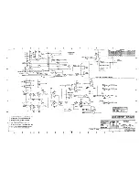
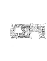
Page 81: ...APPENDIX I PRINTED CIRCUIT BOARD S CHEM A T ICS AND ASSEM B LY DRAW IN G S ...

Page 82: ... IK B UIT A IN 1FFt 05 4 sv 12 9 iO 04 ZS 4 T Eo 5 IJASOJ9 4 TPI I T4 SIT 5 MTIBOFI 11 123 5V I NDEX I I SEI430EI I 032 5 RPZ 4 12 DZTR I 020 5 1300 4 020 lb VM I I I I I I LSOO O R 9 DRSEL t 025 DER DS 2 INDE I l 7 ae DRECIY S 5 V3 ISY I I VPD ZZIC I RPZ 7 1 3 47OIC RPD t5 P R A 5 RIA 47V I I NV ts RP4 47IL 4 TPI2 IZ Q 02TF C 10 L500 IHIFF 9 IO VM 4 IEEADT t I RPS Xn DS I READY I READT INDEX 032 ...

Page 83: ... 2 I 50 NICHE CUVJEMT P SWI7CII R47 3 9KI CRKO 24 ro CIZZI I J ERASE i I LONER HEAD 74LSI4 R49 IK WIZITE EL E CTR O ICG CIZ29 UPPER HEFIID I I CRSO 5V R77 C50 G7OZK o P r x c5 EZK ss G if b NT l R7 br SV IF I I CRZ7 SI I I I I I I I Z R 7E 10 12 R7 oP R C 14 IS C 6 Q 123 55O USO a a CLE 3 RR C 1NT IURT BUSY I Z Sl 754C 2 R79 pRp F Cv I CRZB 5 I ERASE I I s r Ecn 1 HFAD A55Y READ NJC TE I I I I I I...

Page 84: ...PFAO DEl EC 7 EN 5YZ SEI4 II IZV 12V CRIB 470 470 229 AIZY R105 750 C35 229o 5 oK o 95 I R IFo SL09K Iro I 025 I 13 12 RT oZ 750 C41 RCo5 OOI IK ZK14 125 Q IFo 9 lb RCo4 750 ZLKU25 Q16 ZM4125 Q19 CT I CTZI C50 220 5 FAD UO 7 911 1 4 990 RKKo C52 6 LIQ II I o 7 C 10 6 Ul i 221 Q CLR II 12 Broorl SEC 10 0 LIIO o 7o3 R 1 07 9 I5CR 6 C34 ODFV 14 6 Q UI I 22I 5 15 6 2K RBZ 9 36 ip U29 REIXD DATA A CLR ...

Page 85: ...IA ICI I0 38 42 7 OREPig I YPD 2 I C2 22K RP2 I 2 RP3 47OK LI R2 RI SS 2V 4 7 I P UXslC GROUND I I CIIA5515 aeuNTINI PAD C Ill I TP7 P CR I 4 7TEP O IF ov 0 I sf liOEITE I I 150 d RBI v I 2 DR5EL 5 4 88 C II RITE D c poNER C mCTOa P F F ZV SHS i EERIEST L E O WRPRO T 5V 5 RP4 4 7K I IOEITE E PROTECT I s vsv I I t55 I3 C5 4 7 F 50 V ZPL QP Wi ia i4 ID I C a 9 ZZ ZZ ZSZS SI GAS RESIBTi3P ICk RHEO I ...

Page 86: ... w Z2P 220 2124 gl I l I I I I IPUR RI20 41 I I I 71 I LUHI I cRN I I Itl I C4to I I crRY I5LJJ Rl 17 4 714 U3 3 IZ U37 14001 TYP R I IP 4 7 K TIPIIO 4 PL I I f VOTRE COLORS REER I I IQ MQIOR NIZMb OI IORC DR 5E L ID 12 N4 O U35 740 o R130 I K 12 2 14 I U37 SH I D DLDD 5V R99 150 C57 MSEL 9 0 I So ETCH DSN I I I0 12V Z M2901 035 10 12 I I o s U3T Rl IZ 4 7K Rl ll 4 7K C49 C47 C4ED CLGO F P OOl f 1...

Page 87: ...00 0 0 fd 0 dM 9 Sr 3 y 9 IN d MM 5 s m d 5 019f Wme mdl 0 1 e IM M M d M NS M50 VL 00 h r C J M M M BMWMd d Cd jg MSM RWWÃd 9 O I d dp 5 t d 5 Ã4h C M d M V J d 4 m SF SM 5 W M MWeW MM dd TP 90 O P13 fJA e 5 I I 55 05 TB 13 54 y 5 23 k TP1 BBTP I t o 9 5 0 r r s 55 4 0 01 C91 I j J 1 2 1 9 JT i pll P32 JRO CP 0 53 C BOOBJI R O OO 50 1 5 0 f 5 4 2 09 ON O PB R132 Pli O 01OOR 4 4 4 50 1 Q79 d g M Q...

Page 88: ...APPENDIX II RECOM M E N D E D SPARE PARTS LIST ...

Page 89: ...00 21 0084 000 21 0086 000 21 001 1 000 21 0081 000 21 0089 000 210080 000 21 0079 000 21 0083 000 21 0075 000 21 01 24 000 21 0065 001 21 0065 002 21 0090 000 21 01 1 2 000 21 0076 000 2 1 0082 000 21 0036 000 21 01 22 000 Stepper Motor Mounting Assembly Stepper Band Load Power Resistors Diskette Lever Lock Ejector Spring Load Arm Spring Note All components are standard commercial parts purchased...

Page 90: ...Pi N 1 79031 001 1 082 ...

Reviews:

Related manuals for TM848-1