background image

Summary of Contents for 1000 HX

Page 1: ......

Page 2: ...TANDY COMPUTER PRODUCTS TANDY 1000 HX TECHNICAL REFERENCE MANUAL Cat No 25 1513...

Page 3: ...of this manual without express written permission from Tandy Corporation and or its licensor is prohibited While reasonable efforts have been taken in the preparation of this manual to assure its accu...

Page 4: ...ices Power Supply Keyboard Disk Drive Options Important Customer Note A gray stripe has been printed along the right edge of the title page of each of the sections to facilitate your finding the begin...

Page 5: ...TANDY COMPUTER PRODUCTS 1000 HX Main Logic Board...

Page 6: ...n Logic Board 21 Processor Address Data Interface 21 CPU Control Signal Generation 24 IFL Equations 25 System Control Signal Generation 25 Bus Specification 25 Interrupt Function 28 Bus Interface 30 K...

Page 7: ...0 HX will have 640K bytes of RAM allowed by the system memory map Other features include a parallel printer port two built in joystick interfaces and a headphone connection for private listening The M...

Page 8: ...andy 1000 HX The monochrome monitor is a high resolution green phosphor display which provides excellent visual quality It features a 12 screen with an anti glare surface Each display is capable of 25...

Page 9: ...DC 2 0 Amps max 1 2 Amps continuous 12 VDC 1 Amp max Environment Air Temperature System ON 55 to 85 degrees F 13 to 30 degrees C System OFF 40 to 150 degrees F 4 0 to 69 degrees C Humidity System ON O...

Page 10: ...Indicator Keyboard Interface J4 1 2 3 4 5 6 Fan 1 XI X5 X4 X3 X2 X6 12V 2 Ground 2 Gnd 4 NUMLOCK Control 6 CAPS Control 7 XO 8 X7 9 X3 10 XI 11 X5 12 X4 2 GND J5 DC POWER 6 Pin Vertical Header 1 5 VD...

Page 11: ...2 X Axis 3 Ground 4 Switch 1 5 5 VDC 6 Switch 2 J10 3 1 2 Disk Interface Internal Dual 17 Pin Vertical Header 1 3 5 7 9 11 13 15 17 19 21 23 25 27 29 31 33 NC 5 V 5 V 5 V 5 V 5 V Ground Ground Ground...

Page 12: ...A31 NMI D7 D6 D5 D4 D3 D2 Dl DO RDYIN AEN A19 A18 A17 A16 A15 A14 A13 A12 All A10 A09 A08 A07 A06 A05 A04 A03 A02 A01 A00 B01 B02 B03 B04 B05 B06 B07 B08 B09 BIO Bll B12 B13 B14 B15 B16 B17 B18 B19 B2...

Page 13: ...0 Ground 22 Ground 24 Ground 26 NC 28 PPFAULT 30 PPINIT 32 NC 34 5 V Floppy Disk Interface External 1 12V 3 12V 5 GND 7 GND 9 GND 11 GND 13 GND 15 SIDESELECT 17 DIR 19 WRPRT 21 RDDATA 23 WRDATA 25 WEN...

Page 14: ...TANDY COMPUTER PRODUCTS...

Page 15: ...A16 A17 A18 A19 A20 A21 A22 A23 A24 A25 A26 A27 A28 A29 A30 A31 SIGNAL NMI D7 D6 D5 D4 D3 D2 Dl DO READY AEN A19 A18 A17 A16 A15 A14 A13 A12 All A10 A09 A08 A07 A06 A05 A04 A03 A02 A01 A00 IBM Bus Sig...

Page 16: ...rity error information on memory or devices in the I O channel When this signal is active low a parity error is indicated Ready In This line normally high ready is pulled low not ready by a memory or...

Page 17: ...roller This signal is active low FDC DMA Request This line is an asynchronous channel request used by a floppy disk to gain DMA service A request is generated by bringing the line to an active level h...

Page 18: ...TANDY COMPUTER PRODUCTS 12 12Vdc 5 0 1A 12Vdc 10 O 1A GND Ground located on 1 connector pin 0 03A per option board located on 1 connector pin 0 0 3A per option board located on 3 connector pins...

Page 19: ...drive or load characteristics of the signal This includes the specific source by IC type and reference designator drive capability for output signals and actual load for input signals The drive load i...

Page 20: ...duty cycle or 4 77MHz 33 duty cycle SOURCE U23 Drive 75 7 5 UL 14 32MHz 50 duty cycle SOURCE U23 Drive 75 7 5 UL To System NMI Load 1 1 UL U16 SOURCE OPEN COLLECTOR OR 3 STATE BUFFERS Load 1 UL and 1...

Page 21: ...ower REQUEST DMA CHANNEL 0 REQUEST DMA CHANNEL 1 REQUEST DMA CHANNEL 2 REQUEST DMA CHANNEL 3 ACKNOWLEDGE DRQO ACKNOWLEDGE DRQl ACKNOWLEDGE DRQ2 ACKNOWLEDGE DRQ3 TERMINAL COUNT Dedicated input requests...

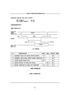
Page 22: ...TANDY COMPUTER PRODUCTS SYSTEM TIMING DIAGRAMS Figure 2 Light Blue to System Timing 1 of 2 17...

Page 23: ...TANDY COMPUTER PRODUCTS Figure 2 Cont Light Blue to System Timing 2 of 2 18...

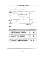
Page 24: ...TANDY COMPUTER PRODUCTS Figure 3 Big Blue to System Timing 1 of 2 19...

Page 25: ...TANDY COMPUTER PRODUCTS Figure 3 Cont Big Blue to System Timing 2 of 2 20...

Page 26: ...sound Processor Address Data Interface The 8088 has three groups of Address Data lines ADO AD7 A8 A15 and A16 A19 ADO AD7 are multiplexed address and data lines To separate and save the address that...

Page 27: ...TANDY COMPUTER PRODUCTS Figure 4 Main Logic Block Diagram 22...

Page 28: ...TANDY COMPUTER PRODUCTS Figure 5 Memory Map 23...

Page 29: ...m C132 which is discharged to 0 volts by diode CR2 when the power is off The READY circuit synchronizes the system ready signals with the CPU clock and generates the CPU input READY If a function need...

Page 30: ...ered by U6 and become IOW f IOR MEMW MEMR f ALE DEN and IO M All external devices except the 8259A Interrupt Controller are buffered by a HCT244 U6 that is controlled by the DEN signal Since the 8259A...

Page 31: ...TANDY COMPUTER PRODUCTS Figure 6 System Control Timing 26...

Page 32: ...TANDY COMPUTER PRODUCTS Figure 7 Expansion I F Connector 27...

Page 33: ...errupts are The NMI interrupt is not maskable by the CPU but it can be enabled disabled by hardware The enable is at Port 00A0 Bit 7 The enable is cleared by RESET There is no specific function assign...

Page 34: ...INTERRUPT CONTROLLER INTERRUPT NMI 0 1 2 3 4 5 6 7 FUNCTION AVAILABLE ON BUS 8253 TIMER CH 0 REFRESH KEYBOARD HARD DISK SECONDARY COMM PRIMARY COMM VERTICAL SYNC FLOPPY DISK CONTROLLER PARALLEL PORT F...

Page 35: ...keyboard data Port B is configured as an output port and is used for control signals for the sound keyboard and timer functions Port C is split into 4 inputs including the timer channel and 2 monitor...

Page 36: ...TANDY COMPUTER PRODUCTS Figure 9 Keyboard Timing Chart 31...

Page 37: ...d circuit and into the 8255 Port C for monitoring by the CPU See Figure 10 Sound Function The sound function consists of an internal and an external sound circuit These are directly connected to the H...

Page 38: ...TANDY COMPUTER PRODUCTS 8253 5 TIMER Figure 10 System Timer 8253 5 33...

Page 39: ...TANDY COMPUTER PRODUCTS Figure 11 Sound Functional Block Diagram 34...

Page 40: ...his comparator output is the X or Y position data bit The ramp is reset to 0 0 VDC whenever a write is made at Port 200 201 Hex The IOW signal turns on Q2 which discharges C129 to 0 0 volts When Q2 is...

Page 41: ...UTER PRODUCTS PROGRAMMING CONSIDERATIONS IOR s REGULAR INTERVALS ONCE TRIGGERED BY SOFTWARE THE INTERGRATOR CIRCUIT PRODUCES A PULSE THE DURATION OF WHICH IS DEPENDENT ON JOYSK POSITION Figure 12 Joys...

Page 42: ...Input Output Output Input Input Input Input Description Raw Clock 16 MHz Write Clock FDC Clock Serial Data From FDD Serial Data From FDC Read Data Window Step Pulses to Move the Head Specifies Seek Mo...

Page 43: ...ller with the F TRKO signal The FDSL also handles DMA Request and Interrupt Enable DMA INTE as well as Interrupt Request INT generated by the FDC Controller The FDSL receives DMA Request DRQ from the...

Page 44: ...orrect set of operating values see Table 2 the address inputs to the dynamic RAMs are generated by a 4 1 multiplexer This MUX switches between video 6845 addresses and CPU addresses as well as between...

Page 45: ...TANDY COMPUTER PRODUCTS Figure 14 Video Controller Block Diagrcun 40...

Page 46: ...TANDY COMPUTER PRODUCTS Figure 15 Video System Memory Map 41...

Page 47: ...Command Hold Time Write Command Hold Time Referenced to RAS Write Command Pulse Width Write Command to Row Strobe Lead Time Write Command to Column Strobe Lead Time Data in Setup Time Data in Hold Tim...

Page 48: ...25 Alpha 71 113 50 59 10 ic 01 19 1A 02 08 06 07 00 00 80 89 16 2b 1 25 26 2 8 6 7 0 0 Low Res Graphics 3b 56 28 2D 08 7F 06 64 70 02 01 06 07 00 00 40 45 8 127 6 100 112 2 1 6 7 0 0 High Res Graphics...

Page 49: ...ny desired organization Normally the pallete is set for a 1 1 mapping red red blue blue etc for PC compatibility However instantly changing the on screen colors is a very powerful tool for animation o...

Page 50: ...Video Reserved Floppy Disk Controller Optional COM Port Not Usable 45 Address 0000 0001 0002 Description DMA Controller IOW 0 Channel 0 Base and Current Address Internal Flip Flop 0 Write A0 A7 Inter...

Page 51: ...p Flop 1 Read A8 A15 DMA Controller IOW 0 Channel 2 Base and Current Word Count Internal Flip Flop 0 Write W0 W7 Internal Flip Flop 1 Write W8 W15 IOR 0 Channel 2 Current Word Count Internal Flip Flop...

Page 52: ...ty 0 Late write selection 1 Extended write selection X If bit 3 1 0 DREQ sense active high 1 DREQ sense active low 0 DACK sense active low 1 DACK sense active high IOR 0 Read Status Register Descripti...

Page 53: ...MA Controller IOW 0f Write Mode Register Description Bitl BitO 0 0 Channel 0 select 0 1 Channel 1 select 1 0 Channel 2 select 1 1 Channel 3 select Bit3 Bit2 0 0 Verify transfer 0 1 Write transfer to m...

Page 54: ...annel 1 mask bit Disable 0 Clear channel 2 mask bit Enable 1 Set channel 2 mask bit Disable 0 Clear channel 3 mask bit Enable 1 Set channel 3 mask bit Disable Don t care IOR Illegal Not Used Descripti...

Page 55: ...fic EOI command Rotate in Automatic EOI Mode set Rotate in Automatic EOI Mode clear Rotate on Specific EOI command Set priority command No operation End of Interrupt End of Interest Automatic Rotation...

Page 56: ...Indicated IR input does not have a slave INITIALIZATION CONTROL WORD 3 Slave Device BitO 2 IDO 2 Bit3 7 0 Not Used INITIALIZATION CONTROL WORD 4 BitO Type of Processor 0 MCS 80 85 Mode 1 8086 8088 Mod...

Page 57: ...ad Counter No 1 8253 5 Timer IOW 0 Load Counter No 2 IOR 0 Read Counter No 2 8253 5 Timer IOW 0 Write Mode Word Control Word Format BitO BCD 0 BCD Counter 4 Decades 1 Binary Counter 16 bits BIT1 3 Mod...

Page 58: ...1 Speaker Data Out Enable 2 Not Used 3 Not Used 4 1 Disable Internal Speaker Sound Control 2 5 0 Not Used 6 0 Not Used 7 1 Keyboard Clear PORT C READ WRITE BITS 4 7 Bits 0 3 READ ONLY 0063 007F Addre...

Page 59: ...Used Not Used WRITE ONLY Description DMA Ch 3 Address A16 DMA Ch 3 Address A17 DMA Ch 3 Address Al8 DMA Ch 3 Address A19 Not Used Not Used Not Used Not Used WRITE ONLY Description DMA Ch 0 1 Address...

Page 60: ...ort 3DEH must be 0 to disable 3B8H and 3BAH Address 00C0 00C7 Bit7 1 0 1 1 0 1 1 0 1 1 1 Bit6 0 X 0 0 X 0 1 X 1 1 1 Bit5 0 FO 0 1 FO 1 0 FO 0 1 1 Bit4 0 Fl 1 0 Fl 1 0 Fl 1 0 1 Bit3 F6 F2 AO F6 F2 AO F...

Page 61: ...epressed R Button 2 Logic 0 Button Depressed L Button 1 Logic 0 Button Depressed L Button 2 Logic 0 Button Depressed Printer Read Status Description Not Used Not Used Not Used 0 Error 1 Printer Select...

Page 62: ...lects 80 by 25 Alphanumeric Mode Graphics Select 0 Selects Alphanumeric Mode 1 Selects 320 by 200 Graphics Mode Black and White 0 Selects Color Mode 1 Selects Black and White Mode Video Enable 0 Disab...

Page 63: ...sed Not Used Not Used Palette Mask 0 Palette Mask 1 Palette Mask 2 Palette Mask 3 Border Blue Border Green Border Red Border Intensity Reserved 0 Mono Enable 1 Reserved 0 Border Enable 4 Color High Re...

Page 64: ...ddress Mode 1 DO Not Used Dl 1 DSO DSO 0 DSO DS2 D2 1 3 Drive Selects DOR Register Write Only BitO 1 Drive Select Bitl BitO 0 0 Drive Select A 0 1 Drive Select B 1 0 Drive Select C Bit2 0 FDC Reset Bi...

Page 65: ...jr 0062 PORT C READ ONLY 1 KEYBOARD LATCHED 0 INTERNAL MODEM INSTALLED 0 DISKETTE DRIVE INSTALLED 0 64K RAM EXPANSION INSTALLED SAME VIDEO SAME KEYBOARD DATA KEYBOARD CABLE INSTALLED TANDY 1000 HX 006...

Page 66: ...12 PC0 PC3 1 CASSETTE MOTOR OFF 0 ENABLE RAM PARITY 0 ENABLE I O CH PARITY 0 HOLD KEYBOARD CLK LOW 0 ENABLE KEYBOARD 1 CLEAR KEYBOARD AND ENABLE CONFIG SW 1 8 IBM PCjr 0061 PORT B READ OR WRITE SAME S...

Page 67: ...0 1 0 1 0 VIDEO SYSTEM MEMORY START ADDRESS 00000 0 20000 128K 40000 256K 60000 324K 80000 512K 00000 0 20000 128K 40000 156K 60000 384K VIDEO SYSTEM MEMORY LENGTH 128K 128K 128K 128K 128K 256K 256K 2...

Page 68: ......

Page 69: ......

Page 70: ......

Page 71: ......

Page 72: ......

Page 73: ......

Page 74: ......

Page 75: ......

Page 76: ......

Page 77: ......

Page 78: ......

Page 79: ......

Page 80: ...TANDY COMPUTER PRODUCTS 1000 HX Devices...

Page 81: ...ntroller intel Floppy Disk Support Motorola Keyboard Interface Motorola 8048 NEC HPD765 FDC NEC Direct Memory Access DMA Tandy Printer Interface Tandy Timing Control Generator Tandy Video Controller T...

Page 82: ...d Unsigned Arithmetic in Binary or Decimal Including Multiply and Divide Two Clock Rates 5 MHz for 8088 8 MHz for 8088 2 Available in EXPRESS Standard Temperature Range Extended Temperature Range The...

Page 83: ...ssing These lines float to 3 state OFF during local bus hold acknowledge S4 0 LOW 0 1 HIGH 1 S6isO LOW S3 0 1 0 1 Characteristics Alternate Data Stack Code or None Data READ Read strobe indicates that...

Page 84: ...imum mode 2 It is used to distinguish a memory access from an I O access IO M becomes valid in the T4 preceding a bus cycle and remains valid until the final T4 of the cycle I O HIGH M LOW IO M floats...

Page 85: ...teristics Interrupt Acknowledge Read I O Port Write I O Port Halt Code Access Read Memory Write Memory Passive The following pin function descriptions are for the 8088 8288 system in maximum mode i e...

Page 86: ...uence of three pulses There must be one idle CLK cycle after each bus exchange Pulses are active LOW If the request is made while the CPU is performing a memory cycle it will release the local bus dur...

Page 87: ...code or data By structuring memory into relocat able areas of similar characteristics and by automati cally selecting segment registers programs are shorter faster and more structured Word 16 bit oper...

Page 88: ...ol signals itself on pins 24 through 31 and 34 The minimum mode 8088 can be used with either a multiplexed or demultiplexed bus The multiplexed bus configuration is compatible with the MCS 85TM multip...

Page 89: ...8088 Figure 5 Multiplexed Bus Configuration 2 67...

Page 90: ...8088 Figure 6 Demultiplexed Bus Configuration Figure 7 Fully Buffered System Using Bus Controller 2 68...

Page 91: ...f a standard 40 lead package The middle eight address bits are not multiplexed i e they remain val id throughout each bus cycle In addition the bus can be demultiplexed at the processor with a single...

Page 92: ...address one or two of the 256 I O byte locations in page 0 of the I O address space I O ports are ad dressed in the same manner as memory locations Designers familiar with the 8085 or upgrading an 808...

Page 93: ...nded to within the limitations of the enable bit and sample period The interrupt return instruction includes a flags pop which returns the status of the original interrupt enable bit when it restores...

Page 94: ...n the address data bus AD0 AD7 at this time into the 8282 8283 latch Address lines A8 through A15 do not need to be latched because they remain valid throughout the bus cycle From T1 to T4 the IO M si...

Page 95: ...al to the equivalent 8086 functions The 8088 handles the external bus the same way the 8086 does with the distinction of handling only 8 bits at a time Sixteen bit operands are fetched or written in t...

Page 96: ...This output occurs on pin 34 in MCS 85 bus structure minimum mode only DT R IO M and SS pro A L E j s d e d b o n e c l o c k e j n t h e m j n j v de the complete bus status in m n mum mode m u m m o...

Page 97: ...0 C TCASE Plastic 0 C to 95 C TCASE CERDIP 0 C to 75 C VCc 5V 10 for 8088 VCc 5V 5 for 8088 2 Symbol V L V H V0L V0H CC LI ILO VCL VCH QN c 0 Parameter Input Low Voltage Input High Voltage Output Low...

Page 98: ...Data in Setup Time Data in Hold Time RDY Setup Time into 8284 Notes 1 2 RDY Hold Time into 8284 Notes 1 2 READY Setup Time into 8088 READY Hold Time into 8088 READY Inactive to CLK Note 3 HOLD Setup...

Page 99: ...Width Address Valid to ALE Low Output Rise Time Output Fall Time 8088 Min 10 10 TCLAX TCLCH 20 TCHCL 10 10 10 TCLCH 30 10 10 10 0 10 10 TCLCL 45 10 2TCLCL 75 2TCLCL 60 TCLCH 60 Max 110 80 80 85 110 1...

Page 100: ...8088 A C TESTING INPUT OUTPUT WAVEFORM A C TESTING LOAD CIRCUIT WAVEFORMS BUS TIMING MINIMUM MODE SYSTEM 2 78...

Page 101: ...mpled near the end of T2 T3 Tw to determine if Tw machines states are to be inserted 3 Two INTA cycles run back to back The 8088 local ADDR DATA bus is floating during both INTA cycles Control signals...

Page 102: ...es 1 2 RDY Hold Time into 8284 Notes 1 2 READY Setup Time into 8088 READY Hold Time into 8088 READY Inactive to CLK Note 4 Setup Time for Recognition INTR NMI TEST Note 2 RQ GT Setup Time RQ Hold Time...

Page 103: ...nactive Delay RD Inactive to Next Address Active Direction Control Active Delay Notel Direction Control nactive Delay Notel GT Active Delay GT Inactive Delay TO Width Output Rise Time Output Fall Time...

Page 104: ...8088 A C TESTING INPUT OUTPUT WAVEFORM A C TESTING LOAD CIRCUIT WAVEFORMS BUS TIMING MAXIMUM MODE SYSTEM 2 82...

Page 105: ...rst and second INTA cycles 4 Two INTA cycles run back to back The 8088 local ADDR DATA bus is floating during both INTA cycles Control for pointer address is shown for second INTA cycle 5 Signals at 8...

Page 106: ...WAVEFORMS Continued ASYNCHRONOUS SIGNAL RECOGNITION BUS LOCK SIGNAL TIMING MAXIMUM MODE ONLY REQUEST GRANT SEQUENCE TIMING MAXIMUM MODE ONLY HOLD HOLD ACKNOWLEDGE TIMING MINIMUM MODE ONLY 2 84...

Page 107: ...8088 8086 8088 Instruction Set Summary All mnemonics copyright Intel Corporation 1987 2 85...

Page 108: ...8088 All mnemonics copyright Intel Corporation 1987 2 86...

Page 109: ...8088 8086 8088 Instruction Set Summary Continued All mnemonics copyright Intel Corporation 19 87 2 87...

Page 110: ...8088 8086 8088 Instruction Set Summary Continued All mnemonics copyright Intel Corporation 1987 2 88...

Page 111: ...l DISP if r m 110 then EA BP DISP if r m 111 then EA BX DISP DISP follows 2nd byte of instruction before data if re quired except if mod 00 and r m then EA disp high disp low if s w 01 then 16 bits of...

Page 112: ...ture Range The Intel 8253 is a programmable counter timer device designed for use as an Intel microcomputer peripher al It uses NMOS technology with a single 5V supply and is packaged in a 24 pin plas...

Page 113: ...us Buffer The 3 state bi directional 8 bit buffer is used to in terface the 8253 to the system data bus Data is transmitted or received by the buffer upon execution of INput or OUTput CPU instructions...

Page 114: ...Word Register The counters are fully independent and each can have separate MODE configuration and counting op eration binary or BCD Also there are special fea tures in the control word that handle th...

Page 115: ...Counter 0 Select Counter 1 Select Counter 2 Illegal RL READ LOAD RL1 RLO 0 1 0 1 0 0 1 1 Counter Latching operation see READ WRITE Procedure Section Read Load most significant byte only Read Load leas...

Page 116: ...the whole process is repeated If the count is odd and the output is high the first clock pulse after the count is loaded decrements the count by 1 Subsequent clock pulses decrement the clock by 2 Afte...

Page 117: ...8253 8253 5 Figure 7 8253 Timing Dlagn 2 19...

Page 118: ...ol word loading as long as the correct number of bytes is loaded in order All counters are down counters Thus the value loaded into the count register will actually be decre mented Loading all zeros i...

Page 119: ...mplete the entire reading procedure If two bytes are programmed to be read then two bytes must be read before any loading WR com mand can be sent to the same counter Read Operation Chart A1 0 0 1 1 AO...

Page 120: ...Ice Parameter Input Low Voltage Input High Voltage Output Low Voltage Output High Voltage Input Load Current Output Float Leakage Vcc Supply Current Min 0 5 2 2 2 4 Vcc 5V 10 Max 0 8 VCc 5V 0 45 10 10...

Page 121: ...ymbol CLK tpWH tpWL GW tGL tGS tGH tOD tODG Parameter Clock Period High Pulse Width Low Pulse Width Gate Width High Gate Width Low Gate Set Up Time to CLKf Gate Hold Time after CLK T Output Delay from...

Page 122: ...8253 9253 5 WAVEFORMS WRITE TIMING READ TIMING CLOCK AND GATE TIMING 2 24...

Page 123: ...he CPU It is cascadable for up to 64 vectored priority interrupts without additional circuitry It is packaged in a 28 pin DIP uses NMOS technology and requires a single 5V supply Circuitry is static r...

Page 124: ...ABLE BUFFER This is a dual function pin When in the Buffered Mode it can be used as an output to control buffer transceivers EN When not in the buffered mode it is used as an input to designate a mast...

Page 125: ...nstruction that is currently being executed and fetch a new routine that will service the requesting device Once this servicing is com plete however the processor would resume exactly where it left of...

Page 126: ...terrupt request lines of lower quality INT INTERRUPT This output goes directly to the CPU interrupt input The VQH level on this line is designed to be fully compatible with the 8080A 8085A and 8086 in...

Page 127: ...8259A Figure 4a 8259A Block Diagram 2 238...

Page 128: ...8259A 2 239 Figure 4b 8259A Block Diagram...

Page 129: ...ase a CALL instruction code 11001101 onto the 8 bit Data Bus through its D7 0 pins 5 This CALL instruction will initiate two more INTA pulses to be sent to the 8259A from the CPU group 6 These two INT...

Page 130: ...irst Interrupt Vector Byte D7 06 D5 D4 D3 D2 D1 00 CALL CODE Figure 5 8259A Interface to Standard System Bus During the second INTA pulse the lower address of the appropriate service routine is enable...

Page 131: ...be brought to a startincyaoint by a sequence of 2 to 4 bytes timed by WR pulses 2 Operation Command Words OCWs These are the command words which command the 8259A to operate in various interrupt modes...

Page 132: ...ant bits of the vectoring byte and the 8259A sets the three least significant bits according to the interrupt level A10 A5 are ignored and ADI Address interval has no effect LTIM If LTIM 1 then the 82...

Page 133: ...ination is by M S M S If buffered mode is selected M S 1 means the 8259A is programmed to be a master M S 0 means the 8259A is pro grammed to be a slave If BUF 0 M S has no function AEOI If AEOI 1 the...

Page 134: ...8259A Figure 7 Initialization Command Word Format Continued 2 245...

Page 135: ...8259A the chip is ready to ac cept interrupt requests at its input lines However during the 8259A operation a selection of algo rithms can command the 8259A to operate in vari ous modes through the O...

Page 136: ...0 indicates the channel is enabled Operation Control Word 2 0CW2 Ft SL EOI These three bits control the Rotate and End of Interrupt modes and combinations of the two A chart of these combinations can...

Page 137: ...RO has the highest prioirity and IR7 the lowest Priorities can be changed as will be explained in the rotating priority mode End of Interrupt EOI The In Service IS bit can be reset either automati cal...

Page 138: ...acknowledged and an End of Interrupt command did not reset its IS bit i e while executing a service routine the 8259A would have inhibited all lower priority requests with no easy way for the routine...

Page 139: ...Register Command is issued with 0CW3 RR 1 RIS 0 The ISR can be read when prior to the RD pulse a Read Register Command is issued with 0CW3 RR 1 RIS 1 There is no need to write an 0CW3 before every sta...

Page 140: ...e of a big system where cascading is used and the priority has to be conserved within each slave In this case the fully nested mode will be programmed to the master us ing ICW4 This mode is similar to...

Page 141: ...the device routine address during bytes 2 and 3 of INTA Byte 2 only for 8086 8088 The cascade bus lines are normally low and will con tain the slave address code from the trailing edge of the first I...

Page 142: ...e reliability D C CHARACTERISTICS TA o C to 70 c vCc 8259A 8259A 2 5V 5 8259A 8 VCc 5V 10 Symbol V L V H V0 L V0 H VOH INT ILI ILOL ex ILIR Parameter Input Low Voltage Input High Voltage Output Low Vo...

Page 143: ...259A 2 TIMING REQUIREMENTS Worst case timing for TCHCL in an actual microprocessor system is typically much greater than 500 ns i e 8085A 1 6 fis 8085A 2 1 AS 8086 1 jms 8086 2 625 ns NOTE This is the...

Page 144: ...8259A A C TESTING INPUT OUTPUT WAVEFORM WAVEFORMS WRITE 2 255 A C TESTING LOAD CIRCUIT...

Page 145: ...8259A WAVEFORMS Continued READ INTA OTHER TIMING 2 256...

Page 146: ...8259A WAVEFORMS Continued INTA SEQUENCE NOTES Interrupt output must remain HIGH at least until leading edge of first INTA 1 Cycle 1 in 8086 8088 systems the Data Bus is not active 2 257...

Page 147: ...TANDY COMPUTER PRODUCTS Floppy Disk Support Chip Specification...

Page 148: ...CTS Floppy Disk Support Chip Specification Contents Section Page General Description 1 Pin Description 2 Block Diagram 3 Environmental Specifications 5 DC Electrical Specifications 5 AC Characteristic...

Page 149: ...write clock to the Floppy Disk Controller Generaters step pulses track 0 indicator DMA request and FDC interrupt signals Generates the Read Data and Read Data Window signals Generates the Write Data...

Page 150: ...250 ns pulse If SWITCH 1 period 1 us 250 ns pulse If SWITCH 0 then CLK16M 4 If SWITCH 1 then CLK16M 2 Serial data from FDD Serial data from FDC Read Data Window Step pulses to move head to another cy...

Page 151: ...TANDY COMPUTER PRODUCTS...

Page 152: ...C 4 5 5 0 5 5 volts VSS 0 0 0 volts ICC milli amps Total Power milli watts 3 2 3 Leakage Current All Inputs Vin 0 0 v 10 micro amps Vin 5 0 v 10 micro amps 3 2 4 Input voltages 3 2 4 1 Except RDDATA T...

Page 153: ...e DMA INTERRUPT Timing IH FIH L L WCK DRQH WCK DRQ DRQH FDRQH DRQ7 FDRQ DIr PDRQr FCKH FDRQH Min 90 100 245 100 20 20 20 20 115 150 275 400 0 750 Typ 120 5 120 250 250 tcr jH Max 130 10 160 255 250 10...

Page 154: ...ng RDAW RDAT RDDH R D D W RDD RDWr RDW ND W U A RDAg RDWC RDDR 11 B RDAg RDWC RDDR ii iii RDAg RDWC RDDH Min 200 188 240 850 3062 15 4812 5062 15 Typ 350 250 875 2 0 Max 30 30 30 30 30 30 550 313 260...

Page 155: ...TANDY COMPUTER PRODUCTS FDSL AC TIMING PIG l FDCCLK FIG 2 WCK FIG 3 WRITE DATA TIMING...

Page 156: ...TANDY COMPUTER PRODUCTS 10 FIG 4 DMA INTERRUPT TIMING...

Page 157: ...TANDY COMPUTER PRODUCTS 11 FIG 5 CONTROL LOGIC TIMING...

Page 158: ...TANDY COMPUTER PRODUCTS FIG 6 DATA SEPARATOR TIMING 12...

Page 159: ...TANDY COMPUTER PRODUCTS Keyboard Interface Chip Specification...

Page 160: ...TANDY COMPUTER PRODUCTS Keyboard Interface Chip Specification Contents Section Page General Description 1 Specifications 3...

Page 161: ...Interface I C provides two funct i ons a Interface between the system I O bus and keyboard b FDC support logic that generates DRIVE SELECT SIGNAL MOTOR ON SIGNAL FDC TERMINAL COUNT FDC RESET and DMA 1...

Page 162: ...t output output output output output output output i nput output output power Keyboard clock Keyboard data K e y b o a r d busy signal Keyboard interrupt signal Monachrame co1 or monitor made Reserved...

Page 163: ...5 Va I ts U R T ground Watts 3 2 D C Electrical Characteristics Symb Parameter Min Typ Max VDD SuppIy Vo Itage 4 5 Icc q Quiescent current Icc o Operating Current Vi I Vih I in Cin Vo I Voh 102 Input...

Page 164: ...TS 3 3 A C E l e c t r i c a l C h a r a c t e r i s t i c s 3 3 1 Ulr i te C y c l e Symb Parameter Tasu Address Setup TWPW Write Pulse Width Tdsu Data Setup Tdh Data Hold Mi n 15 2 A Typ Max Units C...

Page 165: ...TANDY COMPUTER PRODUCTS 3 3 2 Read Cycle 5 OF 5 Symb Parameter Min Typ Max Units Cond Tcspw Chip Select Width 69 nS Trpw Read Pulse Width 6 nS Tda Data Access 6 nS Tdz Bus Hold release 6 25 ns...

Page 166: ...memory 64x8 bits of RAM data memory 27 I O lines an 8 bit interval timer event counter oscillator and clock circuitry The MPD8035HL is intended for applications using external program memory only It...

Page 167: ...stem testing and debugging RD Read RD will pulse low whejijhe processor performs a bus read An active low on RD enables data onto the proces sor bus from a peripheral device and functions as a read st...

Page 168: ...NEC MPD8035HL 48H VDD RAM Power Supply VQDmus tD sett 0 5 V for normal operation VDD sup plies power to the internal RAM during standby mode Vss Ground Vss is ground potential Block Diagram 4 203...

Page 169: ...Max 0 8 0 8 Vcc Vcc 0 45 0 45 0 45 lost V V V V V IOL 2 0 mA V l0L 2 0mA V IOL 2 0 mA DC Characteristics cont TA 0 C to 70 C V c c V D D 5 V 1 0 Parameter Output low voltage all other outputs Output...

Page 170: ...o ALE Port output from ALE Cycle time TO rep rate Symbol tAW tAD1 UD2 UFCI UFC2 l LAFC1 tLAFC2 tCA1 tCA2 trjp tpc tpR tpF trjp IPD tPP tPL tLP tpv tCY tOPRR Min 680 290 40 420 170 120 620 210 460 850...

Page 171: ...tCY 50 1 10 tcv 30 2 5 tC Y 200 3 10 tCY 200 1 3 tCY 150 11 15 tCY 250 8 15 tcY 250 2 15 tC Y 40 1 30 tC Y 40 1 5 tC Y 75 1 10 tCY 75 1 15 tCY 40 4 15 tC Y 40 1 10 tCY 40 4 15 tCY 200 17 30 tCY 120 1...

Page 172: ...tor Logical AND indirect the contents of data memory with accumulator Complement the contents of the accumulator Clear the contents of the accumulator Decimal adjust the contents of the accumulator De...

Page 173: ...he specified register and test contents Jump to specified address if accumulator bit is set Jump to specified address if carry flag is set Jump to specified address if flag FO is set Jump to specified...

Page 174: ...nts of the designated registers into the accumulator Move indirect the contents of data memory location into the accumulator Move contents of the program status word into the accumulator Move immediat...

Page 175: ...contents of flag 1 to 0 Logical AND immediate specified data with contents of bus Logical AND immediate specified data with designated port 1 or 2 Logical AND contents of accumulator with designated p...

Page 176: ...counter output Disable internal interrupt flag for timer counter output Move contents of timer counter into accumulator Move contents of accumulator into timer counter Stop count for event counter St...

Page 177: ...pt In page operation designator Port designator p 1 2 or 4 7 Program status word Register designator r 0 1 or 0 7 Stack pointer Timer Timer flag Testable flags 0 1 External RAM Prefix for immediate da...

Page 178: ...8748 and 8035 processors the PD80C35 PD80C48 features significant savings in power consumption In addition to the power savings gained through CMOS technology the PD80C35 PD80C48 offers two standby mo...

Page 179: ...ata bus Ground Quasi bidirectional port 2 Program output Oscillator control voltage Quasi bidirectional port 1 Test 1 input Primary power supply No connection Pin Functions XTAL1 XTAL2 Crystals 1 2 XT...

Page 180: ...ites data using RD and WR for latching During an external program memory fetch DB0 DB7 output the low order eight bits of the memory address PSEN fetches the instruction DB0 DB7 also output the addres...

Page 181: ...Vrjc 0 3V VS s 0 3toVc c 0 3V 40 Cto 85 C 65 Cto 150 C Comment Exposing the device to stresses above those listed in Abso lute Maximum Ratings could cause permanent damage The device is not meant to b...

Page 182: ...rt 1 port 2 V N V L type0 Port 1 port 2 V N V L type1 SS RESET V N VlL T1 INT VSs V N VCC EA VSS V N VrjC Vss V0 Vcc Bus TO high impedance state VC C 3V VCC 6V tCY 25 MS Halt mode VC C 3V tCY 10MS VCC...

Page 183: ...Input data hold time PROG pulse width Port 2 I O data setup time Port 2 I O data hold time Symbol trjp tpc tpR top tpD tpF tPP tpL tLP Limits 5V 1O Min Max 110 0 80 810 250 65 0 150 1200 350 150 2 5V...

Page 184: ...80C35 C48 PD48 Timing Waveforms Instruction Fetch From External Memory Low Power Standby Operation 1 Halt Mode When El Read From External Data Memory 2 Stop Mode Write to External Memory Port 2 Timing...

Page 185: ...cution when considering interrupt service routine execution following a HALT instruction Figure 1 Stop Mode Circuit RESET Input When a low level input is received by the RESET pin Halt mode is release...

Page 186: ...of the capaci tance and pull up resistance values Figure 3 Stop Mode Control Circuit Port Operation A port loading option is offered at the time of ordering the mask Individual source current requirem...

Page 187: ...equency determined by the resonator or clock source to which it is connected To obtain the oscillation frequency an external LC net work figure 5 may be connected to the oscillator or a ceramic or cry...

Page 188: ...ates the hex number of the specified register or port Program counter Port 1 port 2 or ports 4 7 p 1 2 or 4 7 Program status word Register r 0 7 Symbol SP T TF T0 T1 x x x AND O R EXOR Description Sta...

Page 189: ...ation specified by bits 0 5 of register Rr and the accumulator and stores the result in the accumulator Takes the complement of the contents of the accumulator Clears the contents of the accumulator C...

Page 190: ...ry Exchanges the contents of the lower 4 bits of the accumulator with the upper 4 bits of the accumulator Takes the exclusive OR of immediate data do d7 and the contents of the accumulator and stores...

Page 191: ...flag is not set Jumps to the address specified by ao a7 if the interrupt flag is not set Jumps to the address specified by ao a7 if test 0 is low Jumps to the address specified by ao a7 if test 1 is...

Page 192: ...data memory bank 0 Selects data memory bank 1 by setting bit 4 bank switch of the PSW Specifies data memory 24 31 10 as registers 0 7 of data memory bank 1 Initiates halt mode Moves immediate data do...

Page 193: ...contents of the accumulator into the external data memory location specified by register Rr Exchanges the contents of the accumulator and register Rr Exchanges the contents of the accumulator and the...

Page 194: ...mulator are not changed Takes the logical OR of the contents of the bus and immediate data do d7 and sends the result to the bus Takes the logical OR of the contents of designated port Pp and the lowe...

Page 195: ...f the location specified by the stack pointer executing a return from subroutine with restoration of the PSW Enables internal interrupt of timer event counter If an overflow condition occurs then an i...

Page 196: ...nction equations for those instructions 3 References to addresses and data are specified in byte 1 and or 2 in the opcode of the corresponding instruction 4 The hex value of n for specific registers i...

Page 197: ...age VccOO Cycle Time vs Supply voltage Current Consumption as a Function of Temperature Normal Operating Mode Supply VDttag Vcc V Temperature TA C Supply Current vs Oscillation Frequency 0 1 0 2 0 5 1...

Page 198: ...cont Output High Current vs Output High Voltage Output High Current vs Supply Voltage Output High Current vs Supply Voltage Output Low Current vs Supply Voltage 4 233 Output High Current vs Output Hig...

Page 199: ...PD80C35 C48 juPD48 SEC Operating Characteristics cont 4 234...

Page 200: ...er the DMA or non DMA mode In the non DMA mode the FDC generates interrupts to the processor every time a data byte is to be transferred In the DMA mode the proces sor need only load the command into...

Page 201: ...rotect two side input Ready input Head load output Fault reset step output Low current direction output Read write seek output DC power Pin Functions RESET Reset The RESET input places the FDC in the...

Page 202: ...is 0 low UScUSi Unit Select 0 1 The US0 and US1 outputs select the floppy disk drive unit PSo PSi PreshiftO 1 The PSo and PSi outputs are the write precompensation status for MFM mode They determine e...

Page 203: ...c 5V 5 unless otherwise specified PiranMtcr Input voltage low Input voltage high Output voltage low Output voltage high Input voltage low CLK WR clock Input voltage high CLK WR clock Supply current Vc...

Page 204: ...I delay DACK width TC width Reset width 0O Dr t f tAR tRA tRR tRD tDF l AW tWA tWW tow two tRI twi MCY tAM tMA tAA tTC l RST 40 0 0 250 20 0 0 250 150 5 13 200 2 1 14 125 20 20 200 100 500 500 200 40...

Page 205: ...WR 4 delay from DRQ WE or RD response time from DRQ t tRDW tWRD tus tso tDST STU tSTP tsc tFR l WDD tsu tDS tSTD t DX tMR tMW tMRW 15 15 12 7 1 0 5 0 6 33 8 0 tO 5O 15 30 24 4 800 250 1 15 15 12 7 1...

Page 206: ...SEC MPD765A MPD7265 Timing Waveforms cont Clock DMA Operation FDD Write Operation Seek Operation FLT Reset FDD Read Operation Terminal Count IrVr fe Clock Reset...

Page 207: ...ommand FDD number 1 is in the seek mode If any of the DnB bits is set FDC will not accept read or write command FDD number 2 is in the seek mode If any of the DnB bits is set FDC will not accept read...

Page 208: ...Nam Status Register 1 cont D2 D o ND No Data NW Not Writable MA Missing Address Mark Status Register 2 D7 D6 D5 D4 D3 D2 Di D o CM Control Mark DD Data Error in Data Field w e Wrong Cylinder SH Scan E...

Page 209: ...ymbol Description Namo A0 Address Line 0 C Cylinder Number D Data D7 D0 Data Bus DTL Data Length EOT End of Track Function AQ controls selection of main status register A0 0 or data register Ao 1 C st...

Page 210: ...the main status register selected by A0 0 ST0 ST3 may be read only after a command has been executed and contains information relevant to that particular command Command Symbol Description cont Name...

Page 211: ...MPD765A MPD7265 NEC Table Instruction Set Notes 1 2 cont 12...

Page 212: ...765A MPD7265 Note 1 Symbols used in this table are described at the end of this section 2 AQ should equal 1 for all operations 3 X Don t care usually made to equal 0 13 Table 4 Instruction Set Notes 1...

Page 213: ...se Drive Status Command Result W W W R R W w W W W R 0 X 0 0 0 X 0 X 0 0 SRT 0 X 0 X 0 0 0 X 0 X 0 0 HLT 0 X ST3 0 X 1 0 0 X 1 1 0 USi 0 0 0 1 1 0 HD US i 1 us0 0 1 ND 0 us0 Command codes Head retract...

Page 214: ...ore each byte transfer to the nPD765A PD7265 is required only in the command and result phases and not during the execution phase During the execution phase the main status register need not be read I...

Page 215: ...When sta tus register 0 STO is read after Sense Interrupt Status is issued not ready NR will be indicated The polling of the ready line by the MPD765A MPD7265 occurs con tinuously between commands th...

Page 216: ...ta field are not checked when SK 1 During disk data transfers between the FDC and the processor via the data bus the FDC must be serviced by the processor every 27 s in the FM mode and every 13fiS in...

Page 217: ...ister 1 to a 1 high and terminates the command Status register 0 has bits 7 and 6 set to 0 and 1 respectively Read ID The Read ID command is used to give the present posi tion of the recording head Th...

Page 218: ...the conditions for scan are met then the FDC sets the SH scan hit flag of status register 2 to a 1 high and ter minates the Scan command If the conditions for scan are not met between the starting sec...

Page 219: ...f the seek operation the FDC is in the FDC busy state but during the execution phase it is in the non busy state While the FDC is in the non busy state another Seek command may be issued and in this m...

Page 220: ...the drives A graphic example is shown in figure 4 Figure 4 Seek Recalibrate and Sense Interrupt Status Specify The Specify command sets the initial values for each of the three internal timers The HU...

Page 221: ...st be read When the processor Figure 5 Data Format Sheet 1 of 2 reads status register 0 it will find an 80H indicating an Invalid command was received A Sense Interrupt Status command must be sent aft...

Page 222: ...NEC M P D 7 6 5 A M P D 7 2 6 5 Figure 5 Data Format Sheet 2 of 2 Packaging Information 40 Pin Plastic Package 23...

Page 223: ...and patent indemnification provisions appearing in NEC Electronics Inc Terms and Conditions of Sale only NEC Electronics Inc makes no warranty express statutory implied or by description regarding th...

Page 224: ...TANDY COMPUTER PRODUCTS D M A Chip Specification...

Page 225: ...TANDY COMPUTER PRODUCTS DMA Chip Specification Contents Section Page General Description 1 Address Decode 1 Pin List 5 Pin Functions 6 Logic Block Diagram 10 Electrical Specifications 11 Timing 14...

Page 226: ...ority late write high DREQ sense low DACK sense ADDRESS DECODE MEMORY Provides RAM Memory access decode and address generation Bus addresses A19 A15 determine which segment bank of memory is being acc...

Page 227: ...FOR RAS B 64K DRAMS require address A0 A15 therefore A19 A16 determine access 256K DRAMS require address A0 A17 therefore A19 A18 determine access RAS0B MCF1 MCF0 19 18 17 16 REFRESH MEMRB MEMWB OPTIO...

Page 228: ...combined with Bus strobes I O R B or I O W B to create the chip selects CHIP SELECT FUNCTION DMA DMA SEGMENT REGISTER ADDRESS SIGNAL EQUATION A19 A16 don t care A15 A8 0 ALWAYS X 0000 X 000F DMACSB A...

Page 229: ...he bi directional data buffer Since it must be shared by the memory this part will be provided externally Decoding from the ADDRESS DECODE I O and MEMORY circuitry are combined to provide directional...

Page 230: ...TANDY COMPUTER PRODUCTS PIN LIST...

Page 231: ...EMWB MEMRB IOWB IORB D7 D6 D5 D4 D3 D2 Dl DO PIN NUMBER 1 2 3 4 5 6 7 8 9 10 11 12 13 14 15 16 17 18 19 20 21 22 23 24 25 26 27 28 29 30 31 32 33 34 FUNCTION VDD CASB RASOB RAS1B RAS2B MAO MAI MA2 MA3...

Page 232: ...ardware master RESET OSC Memory timing clock Currently CLK14M AEN CPU Bus Grant 8237 HLDA TEST Input for TEST mode used by IC mfg BI DIRECTIONAL 32 pins BUSA19 BUSA16 System Segment Address CPU BUS MA...

Page 233: ...Acknowledge from DMA channel 0 setup for refresh 8237 CHANNEL 1 ACKNOWLEDGE DREQl 8237 CHANNEL 2 ACKNOWLEDGE DREQ2 8237 CHANNEL 3 ACKNOWLEDGE DREQ3 8237 EOP output only CPU Bus Request 8237 HRQ 5 VDC...

Page 234: ...MA PINOUT DO Dl D2 D3 D4 D5 D6 D7 MADO MAD1 MAD2 MAD3 MAD4 MAD5 MAD6 MAD7 MAD 8 RESET READY DMATC BREQ OSC DRQ3 FDCDMARQ DRQ1 RFSH REFRESH DACK1 FDCDMACK DACK3 RASO RAS1 RAS2 CAS WR MCF1 MCFO DBDIR DB...

Page 235: ...TANDY COMPUTER PRODUCTS LOGIC BLOCK DIAGRAM 10...

Page 236: ...OPERATING AMBIENT MIN TYP MAX UNITS AIR TEMP RANGE 0 25 70 DEGREES C POWER SUPPLIES VDD 4 5 5 0 5 5 VOLTS VSS 0 0 0 VOLTS ICC 100 MILLIAMPS NOTE INCLUDE ALL RELEVENT CONDITIONS UNDER WHICH ICC IS TO...

Page 237: ...S LOGIC 0 Vol 0 4 volts 4 0 MA LOAD LOGIC 1 Voh 2 4 volts 0 4 MA LOAD INPUT CAPACITANCE MIN TYP MAX All inputs 0 0 Vin 5 0 10 picofarads OUTPUT CAPACITANCE All outputs 50 picofarads Except Data bi dir...

Page 238: ...N MAXIMUM LOADING FOR EACH OUTPUT Capacitive Load 50pf Current Load Ioh 4 0 MA Iol 0 4 MA INPUT OUTPUT TIMING NOTE ALL AC TESTING AND TIMING MEASUREMENTS WILL BE AT THE FOLLOWING CONDITIONS VOH OUTPUT...

Page 239: ...TANDY COMPUTER PRODUCTS Figure 1 MEMORY TIMING PARAMETERS READ 14...

Page 240: ...Delay after DBDIR hi DBENB Hold from STROBE hi DBDIR Hold from DBENB hi min 50 15 don t 0 0 100 0 75 20 20 35 70 0 0 0 typ 69 8 250 250 care 69 8 69 8 150 70 max 40 40 40 70 70 40 NOTE NOTE NOTE NOTE...

Page 241: ...TANDY COMPUTER PRODUCTS Figure 2 MEMORY TIMING PARAMETERS WRITE 16...

Page 242: ...ATA Valid Hold after STROBE hi tl3 WRB lo Setup to CASB lo tl4 WRB lo Hold after CASB lo tl5 DBENB lo Delay after STROBE lo tl6 DBENB Hold from STROBE hi min typ max I 50 20 30 70 70 NOTE 1 1 2 3 3 1...

Page 243: ...BE lo STROBE lo Setup to OSC hi STROBE lo Length STROBE hi Setup to OSC hi DATA Valid Setup to STROBE hi DATA Hold from STROBE hi DBDIR hi Delay from STROBE lo DBENB lo Delay after DBDIR hi DBENB Hold...

Page 244: ...SELECT PARAMETERS WRITE min typ max tl ADDRESS Valid Setup to STROBE lo t2 STROBE lo Setup to OSC hi t2A STROBE lo Length t3 STROBE hi Setup to OSC hi t4 DATA Valid Setup to STROBE lo t5 DATA Hold fr...

Page 245: ...TANDY COMPUTER PRODUCTS Figure 5 DMA BUS MASTER TIMING READ WRITE 20...

Page 246: ...e DACK B False delay from CLK lo ADDRESS Valid Setup to CLK Hi ADDRESS False delay from CLK hi tl2 MEMRB or IORB True Delay from CLK hi tl3 MEMRB or IORB False Delay after CLK hi tl4 MEMWB or IOWB Tru...

Page 247: ...TANDY COMPUTER PRODUCTS Printer Interface Chip Specification...

Page 248: ...TANDY COMPUTER PRODUCTS Printer Interface Chip Specification Contents Section Page General Description 1 Specifications 3...

Page 249: ...t e r I n t e r f a c e i C p r o v i d e s t h e i n t e r f a c e b e t w e e n t h e s y s t e m I O b u s a n d t h e p r i n t e r F i g u r e 1 s h o w s B l o c k d i a g r a m o f P r i n t e...

Page 250: ...wer Descr i pt i on Interrupt signal Switch for totem pole output or open col lector output an INITB AF STROBEB CPU address 1 i ne CPU address 1 i ne Data I O 1 i ne Data I O 1 i ne Data I O 1 i ne Da...

Page 251: ...ion 0 5 Uatts 3 2 D C E l e c t r i c a l C h a r a c t e r i s t i c s 3 OF 5 Symb VDD Icc q Icc o Vi 1 Vi h I in Cin Vol Voh IDZ Parameter Supp1 y Vo 1tage Quiescent current Operating Current Input...

Page 252: ...TS 3 3 A C E l e c t r i c a l C h a r a c t e r i s t i c s 3 3 1 W r i t e C y c l e Symb Parameter Tasu Address Setup Twpw Write Pulse Width Tdsu Data Setup Tdh Data Hold 4 OF 5 Mi n 15 TyP Max Un...

Page 253: ...TANDY COMPUTER PRODUCTS 5 OF 5 3 3 2 R e a d C y c l e Symb Tcspw Trpw Tda Tdz Parameter Chip Select Width Read Pulse Width Data Access Bus Hold release Min Typ Max 25 Un i ts Cond nS nS nS ns...

Page 254: ...TANDY COMPUTER PRODUCTS Timing Control Generator Chip Specification...

Page 255: ...TANDY COMPUTER PRODUCTS Timing Control Generator Chip Specification Contents Section Page General Description 1 Block Diagram 3 Specifications 4 Timing Diagrams 5...

Page 256: ...s interfaces the system signals HOLD HLDA with the CPU s ignals RQ GT creates two FDC chip selects and the DMA request deI ay 1 2 3 4 5 6 7 a 9 1 0 1 1 1 2 13 1 4 15 1 6 17 1 8 19 2 0 VIDLJAITB FAST D...

Page 257: ...ait Clock speed select CLK477M 4 Squarewave FDC DMA Request Beginning of FDCDRQ delayed 1 0 microsec System Address Address Latch Enable Data Enable I O Wr i te I O Read 0SC16M 2 Squarewave 0SC28M 2 S...

Page 258: ...TANDY COMPUTER PRODUCTS...

Page 259: ...perating Ambient Air Temp Range D 25 70 degrees C 3 2 2 Power Supplies VDD 4 5 5 0 5 5 volts VSS 0 0 0 volts ICC 100 m i I I i amps Total Power 700 milliwatts 3 2 3 Leakage Current All Inputs Vin 0 0...

Page 260: ...to 4 0v tF fal1 time 4 0 to 0 4v tCYC 7 IS MHZ min typ max 44 69 5 tR tF 68 69 5 8 7 140 4 77MHZ min typ max 1 69 69 5 ns 1 118 140 tR tF ns 1 10 ns 1 10 ns 1 210 ns FIGURE 1 CPUCLK FIGURE 2 RESET RES...

Page 261: ...False False False True True True True Setup to CPUCLK low Hold after CPUCLK low before CPUCLK low Hold after CPUCLK hi Setup to CPUCLK hi Hold after CPUCLK low before CPUCLK low Hold after CPUCLK hi...

Page 262: ...ROL GENERATOR CONTROL GENERATOR tl STATUS Active Delay from CLK hi t2 STATUS Inactive Delay from CLK low t3 ALE True Delay from Status Active 1 m1n I 10 1 10 1 max 60 70 20 ns tCHSV 8088 ns tCLSH 8088...

Page 263: ...from CLK low STROBE False Delay from CLK hi STROBE True Delay from Clk hi I I 55 1 1 1 1 20 30 30 30 30 ns ns ns ns ns ns ABRITTER PARAMETER tl HOLDB True setup to CPUCLK low t2 CPUCLK low to RQ GTB...

Page 264: ...PUCLK low ACK pulse 1 lay 1 to CPUCLK low 1 20 20 50 ns ns 50 ns 30 ns ns tCHGX 8088 tCLGL 8088 tCLGH 8088 CLOCK PARAMETER tl t2 t3 t4 t5 t6 t7 t8 OSC28M Period CLK14M Period CLK14M high Includes tRIS...

Page 265: ...enerates FIGURE 7 OSCILLATOR CLOCK RELATIONSHIPS 8MHZ t9 CLK3580K low Includes tFALL tR CLK M tF CLK M 1 t7 t8 1 1 10 ns 10 ns CLOCK PARAMETER tl OSC16M Period t2 CLK8M Period t3 CLK8M High includes t...

Page 266: ...tR tF FIGURE 8 FDCCLK FDWCK RELATIONSHIPS 10 ns 10 ns CLOCK PARAMETER tl FDCWCK High Includes tRISE t2 FDCWCK Period 1 1 min 1 1 typ 250 2 J0T max ns us FIGURE 9 CLK4M FDDMAREQ RELATIONSHIPS...

Page 267: ...CLOCK PARAMETER tl t2 t3 FDCDRQ Setup DFDCDRQ Delay FDCDRQ False to CLK4M TRUE to DFDCDRQ False Delay 1 1 1 1 1 ml n 20 75 us typ 1 2 us max 1 1 20 ns us ns Asynchronous...

Page 268: ...TANDY COMPUTER PRODUCTS Video Controller Chip Specification...

Page 269: ...COMPUTER PRODUCTS Video Controller Chip Specification Contents Section Page General Description 1 Block Diagram 2 Operating Modes 3 Pin List 24 Logic Block Diagram 27 Electrical Specifications 29 Timi...

Page 270: ...for a number of video modes These modes use varying numbers of colors 2 4 or 16 These 16 colors are defined by combinations of the RGBI as shown in the color chart below and can be used for the foregr...

Page 271: ...TANDY COMPUTER PRODUCTS Figure 1 VIDEO CONTROLLER CHIP BLOCK DIAGRAM...

Page 272: ...ers 16 Special Graphics characters 32 Word Processing Scientific Notation characters In both modes all characters are 7 dots wide by 7 dots high and are placed in an 8 dot wide by 8 or 9 dot high matr...

Page 273: ...Medium Resolution 320 x 200 X 16 Color Low Resolution 160 x 200 X 2 Color High Resolution 640 x 200 X 4 Color High Resolution 640 x 200 X IBM PC X GRAPHICS MEMORY USAGE 200 line Graphics Memory uses e...

Page 274: ...high resolution monitor for proper operation Available in the IBMPC and IBM PCjr this mode has the following characteristics Contains a maximum of 200 rows of 640 PELs Can display 2 of 16 possible co...

Page 275: ...of 200 rows of 640 PELs Can display 4 of 16 possible colors Each pixel selects 1 of 4 colors Requires 32K bytes of read write memory Formats 8 PELs per two bytes 1 even byte and 1 odd byte in the foll...

Page 276: ...er byte in the following manner 7 PA3 6 PA2 5 PAl 4 PA0 3 PA3 2 PA2 1 PAl 0 PA0 First Display PEL Second Display PEL 16 COLOR LOW RESOLUTION 160 X 200 GRAPHICS MODE The 16 Color Low Resolution 160 X 2...

Page 277: ...6K bytes of read write memory Formats 4 PELs per byte in the following manner 7 PA1 6 PA0 5 PAl 4 PA0 3 PAl 2 PA0 1 PAl 0 PA0 First Display PEL Second Display PEL Third Display PEL Fourth Display PEL...

Page 278: ...The following registers can be accessed by writing their Hex Address to 3DA and their Data to 3DE Hex Address 01 02 03 10 lF Video Array Register Palette Mask Border Color Mode Control Palette Registe...

Page 279: ...TANDY COMPUTER PRODUCTS ARRAY BORDER COLOR 10...

Page 280: ...TANDY COMPUTER PRODUCTS ARRAY MODE CONTROL REGISTER 11...

Page 281: ...this section Note The palette address can be masked by using the palette mask register The following is a description of the register s bit functions Bit Number Function 0 Blue 1 Green 2 Red 3 Intensi...

Page 282: ...logic PALETTE ADDRESS BITS 13 PA1 0 0 1 1 PAO 0 1 0 1 Function Palette Register 0 Palette Register 1 Palette Register 2 Palette Register 3 PA3 I 0 0 0 0 0 0 0 0 1 1 1 1 1 1 1 1 PA2 R 0 0 0 0 1 1 1 1...

Page 283: ...TANDY COMPUTER PRODUCTS DETAILED I O REGISTER INFORMATION 14...

Page 284: ...TANDY COMPUTER PRODUCTS 15...

Page 285: ...TANDY COMPUTER PRODUCTS 16...

Page 286: ...TANDY COMPUTER PRODUCTS 17...

Page 287: ...TANDY COMPUTER PRODUCTS 18...

Page 288: ...TANDY COMPUTER PRODUCTS Bit Progranuning 19...

Page 289: ...TANDY COMPUTER PRODUCTS 20...

Page 290: ...21 1 0 1 2 3 4 5 6 7 8 9 10 11 12 13 REGISTER Horizontal Total Horiz Displayed Hor i z Sync Pos Horiz Sync Width Vertical Total 1 Vert Total Adjust Vertic Displayed Vert Sync Pos Interlace Mode MaxSca...

Page 291: ...0 0 0 9 F F F F 0 0 0 0 0 3 F F F F 2 0 0 0 0 5 F F F F 4 0 0 0 0 7 F F F F 6 0 0 0 0 9 F F F F VIDEO MEMORY ADDRESSING MODES 22 H3DD BIT 0 EXTADR 0 0 0 0 1 1 H3DF BIT 7 ADRM1 0 0 1 1 0 0 H3DF BIT 6...

Page 292: ...BELOW 1 1 1 1 1 1 1 0020 0027 0040 0047 0060 0067 0200 0207 00C0 00C7 03F0 03F7 0378 037F DESCRIPTION INTCSB TMRCSB PIOCSB JOYSTKCSB SNDCSB FDCCSB PRINTCSB The output signal ROMIOSELB is the enable s...

Page 293: ...TANDY COMPUTER PRODUCTS PIN LIST 24...

Page 294: ...0 External Memory Data I O Bank 0 External Memory Data I O Bank 1 External Memory Data I O Bank 1 External Memory Data I O Bank 1 External Memory Data I O Bank 1 External Memory Data I O Bank 1 Extern...

Page 295: ...ut Output Output Output Output Output Output Output Input Output Input Output Green Video Out Monochrome Video CPU Address Line CPU Address Line CPU Address Line CPU Address Line CPU Address Line CPU...

Page 296: ...bits of the BA lines according to the following chart TEST MODE 1 2 3 4 ENABLED WHEN BMEMRB 0 0 0 0 BMEMWB 0 0 0 0 BA15 1 0 0 0 BA14 X 1 X X BA13 X X 1 X BA12 X X X 0 1 OPERATION PERFORMED Pinout the...

Page 297: ...LB A B C COMPSYNC COMPCOLOR IOMB See Note BIOWB RFSHB BAEO LPSWB Not Used DB 7 0 RASB CASB OUTR OUTI MWEOB OUTHSYNC OUTVSYNC Also the Pass Fail bit for the Self Test ROM can be tested on the OUTG outp...

Page 298: ...CURRENT MIN 0 4 5 0 TOTAL POWER DISSIPATION INCLUDE LOADING ON OUTPUTS LEAKAGE CURRENT ALL INPUTS AND TRISTATE OUTPUTS INPUT VOLTAGES LOGIC 0 Vil ALL INPUTS LOGIC 1 Vih ALL INPUTS MIN 10 2 0 TYP 25 5...

Page 299: ...TIMING 1 1 1 1 1 1 1 1 1 2 1 3 4 5 DESCRIPTION ADDRESS VALID TO BIORB ACTIVE SETUP ADDRESS VALID HOLD AFTER BIORB INACTIVE BIORB PULSE WIDTH LOW BIORB ACTIVE TO DATA OUT VALID MIN 1 50 1 50 250 1 BIOR...

Page 300: ...9 DATA IN VALID TO 10 BIOWB INACTIVE TO 11 ADDRESS VALID TO C 12 ADDRESS NOT VALID 13 BIOWB INACTIVE TO LOW BIOWB INACTIVE DATA IN VALID BrA ROMIOSELB MIN MAX UNITS NOTE 1 501 INACTIVE 50 SETUP HOLD...

Page 301: ...TANDY COMPUTER PRODUCTS MEMORY DECODE TIMING MEMORY READ OR WRITE OPERATION 32...

Page 302: ...D TO ROMIOSELB INACTIVE OUT DELAY 2O VIDWAIT DELAY FROM BMEMRB READ LOW 211 22 23 24 25 26 27 VIDWAIT PULSE WIDTH XMD YMD SETUP TO CASB LOW MEM READ XMD YMD HOLD TO CASB LOW MEM READ VIDWAIT LOW DELAY...

Page 303: ...TANDY COMPUTER PRODUCTS CRTC TIMING 34...

Page 304: ...0 4 delay time CLK fall to HS VS DE CURSOR delay time MA 7 0 BANKSL setup to RASB low MA 7 0 BANKSL setup to CASB low MA 7 0 BANKSL hold from RASB low MA 7 0 rBANKSL hold from CASB low RASB CASB fall...

Page 305: ...aracteristics Relative Skew of R G B I Relative Skew of R G B I With respect to Compcol Relative Skew of R G B I With respect to CompSync OutHsync OutVsync Relative Skew of R G B I With respect to Com...

Page 306: ...Programmable Vertical Sync pulse width standard for S version optional for R Rl and SY versions o Row Column display memory addressing SY version o Double Width character control OPTIONAL FEATURES o...

Page 307: ...e Specify READ high or WRITE low operation Chip 6845 megacell select low true Character Clock Not Used Data Bus Raster Address Horizontal Sync Reset low true Signal DE CURSOR VS I O OP OP OP Descripti...

Page 308: ...AENB 0 the MA outputs are enabled AENB 1 forces the MA outputs into a high impedance state 14 15 or 16 bit Advanced Memory Address bus separate video memory address information on this bus precedes t...

Page 309: ...45SY IP One of these three inputs is tied high to select the version of the VE68C45 used in your application The remaining two inputs must be grounded NOTE the VE68C45SY does not provide 6545 transpar...

Page 310: ...DC characteristics Ta 0 70 degree C Vss 0vf Vcc 5 Characteristics Symbol Min Typ Max Units Input High Voltage Inputs 1 0 Input Low Voltage Inputs 1 0 Output High Voltage Outputs 1 0 Output Low Voltag...

Page 311: ...TANDY COMPUTER PRODUCTS AC CHARACTERISTICS Vcc 5v 10 r Vss 0v Ta 0 C t o 70 C VTI BUS TIMING 42...

Page 312: ...WRITE TANDY COMPUTER PRODUCTS 43...

Page 313: ...N read write to enable set up TENW enable pulse width TENA enable to address hold time TENC enable to cs hold time TENRW enable to read write hold time read TEND enable to read data delay TENDF enable...

Page 314: ...22 23 24 Characteristics CLK frequency CLK width CLK rise and fall time CLK fall to MAO 15 RA0 4 delay time CLK fall to HS VS DE CURSOR delay time Symbol Fcyc PWcl Tcr Tcf TmadfTrad Thsd Tvsd Tdtd Tcd...

Page 315: ...NCR MICROELECTRONICS DIVISION NCR 8496 SOUND GENERATOR DATA SHEET...

Page 316: ...Circuitry INTERFACE DEFINITIONS 3 1 Microprocessor Interface 3 2 Audio Application Interface 3 3 Power Interface ELECTRICAL CHARACTERISTICS 4 1 Operating Conditions 4 2 Input Characteristics 4 3 Outpu...

Page 317: ...FEATURES Functionally and Pin compatible with the SNR76496 Programmable white or periodic noise generator Three programmable tone generators Programmable attenuation values Simultaneous multiple sound...

Page 318: ...NCR 8496 FUNCTIONAL BLOCK DIAGRAM...

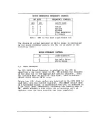
Page 319: ...ation Tone 3 Frequency Tone 3 Attenuation Noise Control Noise Attenuation Note RO is the most significant address bit 2 2 Tone Generation The NCR 8496 sound generator has three 3 programmable tone gen...

Page 320: ...1 1 A3 0 1 0 1 0 1 0 1 Value dB 0 2 4 6 8 10 12 14 AO 1 1 1 1 1 1 1 1 Al 0 0 0 0 1 1 1 1 Data A2 0 0 1 1 0 0 1 1 A3 0 1 0 1 0 1 0 1 Value dB 16 18 20 22 24 26 28 OFF Note AO is the most significant b...

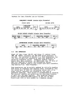
Page 321: ...The NCR 8496 Sound Generator is_enabled by the CPU by asserting a low logic level to CE WE strobes the contents of the data bus to the appropriate control register Data bus contents must be_valid at t...

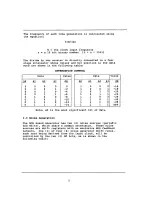
Page 322: ...data are required by each tone generator in selecting frequency values Frequency updates require double byte data transfers An additional four 4 bits of data are required to select the attenuation val...

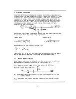
Page 323: ...pled into the application audio circuit via a filtering network similar to the following The upper and lower frequency poles for the application are determined from the following equations Typically R...

Page 324: ...t state until READY is true INPUT Write Enable WE indicates that data is available to the NCR 8496 when true low INPUT Chip Enable CE indicates that data may be transferred to the NCR 8496 INPUT Maste...

Page 325: ...ignal vcc GND Pin 7 9 INTERFACE Pin 16 8 Description OUTPUT Audio signal to application Refer to section 2 6 Output Circuitry for recommended output connections INPUT Audio input signal from applicati...

Page 326: ...Maximum Symbol v cc J cc T o T s vmax Conditions Outputs Open To Any Pin Min 4 5 0 65 Max 5 5 40 70 150 7 0 Units V mA C C V 4 2 INPUT CHARACTERISTICS Parameter Input Voltage Low Input Voltage High In...

Page 327: ...Bias Voltage Symbol 0 0 V 0Q V 0M V SW C 0L Conditions Causing half scale output swing Over Output Voltage Swing Over Output Voltage Swing Generators at OdB Generators at OdB From Pin 7 to Ground for...

Page 328: ...Parameter CE READY Frequency Input Set up Time Hold Time Symbol fc CER CLOCK t sul Conditions CL 225pf RL 2K to VCC Transition Time Data WE CE WE Data READY Min 05 0 0 Max 150 4 Units nS MHz nS nS DAT...

Page 329: ...TANDY COMPUTER PRODUCTS 1000 HX Power Supply Single and Dual Input...

Page 330: ...TANDY COMPUTER PRODUCTS 1000 HX 28 Watt Single Input Power Supply...

Page 331: ...TANDY COMPUTER PRODUCTS 1000 HX 28 Watt Single Input Power Supply Contents Section Page Operating Characteristics 1 Block Diagram 2 Theory of Operation 3 Schematic 5...

Page 332: ...t Noise Vol Vo2 Vo3 Efficiency Holdup Time Pull Load at Nominal Line Insulation Resistance Input to Output Input to Ground Isolation Input to Ground MINIMUM 90 47 4 85 11 40 13 20 1 25 0 1 0 5 8 65 16...

Page 333: ...Power Supply Block Diagram...

Page 334: ...sistor Ql is On the Ql current excites the transformer Tl and voltage rises in the bias coil of TK5 6 which leads transistor Ql positive bias then transistor Ql turns ON When transistor Ql turns ON co...

Page 335: ...Photo coupler isolates the primary and secondary circuits Over Voltage Protection When the 5 output voltage rises between 5 8V to 6 8V the 12V circuit will be shorted by the Thyristor SCRl under the c...

Page 336: ......

Page 337: ...TANDY COMPUTER PRODUCTS 1000 HX 28 Watt Dual Input Power Supply...

Page 338: ...TANDY COMPUTER PRODUCTS 1000 HX 28 Watt Dual Input Power Supply Contents Section Page Operating Characteristics 1 Block Diagram 2 Theory of Operation 3 Schematic 5...

Page 339: ...3 Efficiency MINIMUM 90 198 47 4 85 11 40 13 20 1 25 0 1 0 5 8 Holdup Time Full Load at Nominal Line 16 Insulation Resistance Input to Output Input to Ground Isolation Input to Ground Input to Output...

Page 340: ...Power Supply Block Diagram...

Page 341: ...sistor Ql is On the Ql current excites the transformer Tl and voltage rises in the bias coil of TK5 6 which leads transistor Ql positive bias then transistor Ql turns ON When transistor Ql turns ON co...

Page 342: ...Photo coupler isolates the primary and secondary circuits Over Voltage Protection When the 5 output voltage rises between 5 8V to 6 8V the 12V circuit will be shorted by the Thyristor SCRl under the c...

Page 343: ......

Page 344: ...TANDY COMPUTER PRODUCTS 1000 HX 25 6 Watt Power Supply...

Page 345: ...TANDY COMPUTER PRODUCTS 1000 HX 25 6 Watt Power Supply Contents Section Page Specifications 1 Block Diagram 4 Theory of Operation 5 Schematic 9...

Page 346: ...o3 12 0 VDC 10 13 2 to 10 8 VDC OUTPUT RIPPLE AND NOISE VOLTAGE OUTPUT RIPPLE AND NOISE VOLTAGE Vol 5V 50mV p p Vo2 12V lOOmV p p Vo3 12V 150mV p p Note Ripple is defined as a composite of a power lin...

Page 347: ...shall be 600 millivolts and of the positivre five volt output shall be 150 millivolts OUTPUT HOLDUP TIME Nominal Line 16msec min Low Line 10msec min OUTPUT CURRENT OUTPUT MINIMUM LOAD MAXIMUM LOAD Vo...

Page 348: ...uting device with 3dB margin at 450 kHz increasing linearly to 8dB margin at 1 0 MHz and with 8dB margin from 1 0 to 30 MHz Line conducted noise is measured at the operating AC input for all output lo...

Page 349: ...POWER SUPPLY BLOCK DIAGRAM...

Page 350: ...ON When transistor Ql is set to ON the Ql current excites transformer Tl and the voltage rises in the bias coil of Tl 4 5 which leads transistor Ql positive bias then transistor Ql turns ON When the t...

Page 351: ...ltage are represented by the following equations Vo n x Vf Vo Output Voltage n Turn ratio of transformer Tl Vf Collector voltage at turn off time Vin x Ton Vf x Toff Vin Input voltage Ton Turn on time...

Page 352: ...ne input voltage which feeds back to the control circuit through a photo coupler to keep the output voltage stable Over Voltage Protection When the output voltage is 5 8V to 6 8V the 12V circuit is sh...

Page 353: ...model no 8 7 9 0 0 9 3...

Page 354: ...TANDY COMPUTER PRODUCTS 1000 H X Keyboard...

Page 355: ...TANDY COMPUTER PRODUCTS 1000 HX Keyboard Contents Section Keyboard Specificatins Keyboard Circuit Keyboard Key Layout Page 2 5 7...

Page 356: ...TANDY COMPUTER PRODUCTS SPECIFICATION NON ENCODED KEYBOARD MATRIX REV A 12 18 35 REV B 2 11 36 SEE SHEET 1A FOR REVISIONS...

Page 357: ...5 ADDED SPLIT CABLE OPTION AND INCREASED OVERALL WIDTH MOUNTING DIMS DWG WAS 8010010 1 10 86 DELETED SINGLE CABLE OPTION CHG D 8 12 POSITION CABLES TO 12 13 POSITION CABLES RESPECTIVELY 2 20 86 SPACE...

Page 358: ...or 1 minute betweem PCB pattern and iron panel 150 Vdc for 1 minute between switch contacts 3 Mechanical Characteristics 3 1 Operating Force s 70g 25g at full stroke at center of keycap 3 2 Plunger St...

Page 359: ...5 Vibration 10 to 55 Hz 1 5mm along each of the orthogonal axis 5 6 Shock s 50G 11 msec 1 2 sine wave 3 directions each 3 times 6 Safety Standards Keyboard must meet UL standard 114 CSA SPEC C22 2 NO...

Page 360: ...rinted flat on the keycaps as they appear on the D size drawing Two shot molding or sublimation printing is preferred 8 Drawings 8 1 Mechanical Specifications Keytop Arrangement D 8080079 Sheets 6 and...

Page 361: ......

Page 362: ......

Page 363: ...TANDY COMPUTER PRODUCTS 1000 HX Disk Drive...

Page 364: ...TANDY COMPUTER PRODUCTS 1000 HX Disk Drive Contents Section Page Specifications 1 Exploded View 23 Schematics 25...

Page 365: ...le Sided 80 Tracks Recording Capacity IMBytes Transfer Rate 250 Kbits sec TTL interface without Ready signal VALID for MP F63W 72D with the following serial numbers SONY CORPORATION MFD TECHNICAL INFO...

Page 366: ...onsumption 2 4 2 Supply Voltages 2 5 Environmental Limits and Orientation 2 5 1 Temperature 2 5 2 Humidity 2 5 3 Vibration 2 5 4 Shock 2 5 5 Orientation 3 Interface 3 1 Pin Assignment 3 1 1 Signal Con...

Page 367: ...ower On Initialization 6 Test Points Page 3 3 4 Timing Requirements 3 3 1 3 3 2 3 3 3 3 3 4 3 3 5 3 3 6 3 3 7 3 3 8 3 3 9 3 3 10 3 3 11 3 3 12 DRIVE SELECT 0 lf2f3 MOTOR ON STEP DIRECTION HEAD SELECT...

Page 368: ...media or any other ANSI specification media agreed upon by Sony and the drive customer 2 Specifications 2 1 Configuration The drive consists of Read Write heads head positioning mechanism disk motor...

Page 369: ...MP F63W 70D Figure 2 1 PHYSICAL DIMENSIONS Page 5...

Page 370: ...s the disk is kept inserted 2 3 4 Functional a Rotation Speed 300 rpm The continuous speed variation is within 1 5 The instantanuous speed variation is within 1 0 b Recording Density 8717 BPI Side 1 T...

Page 371: ...60 C 20 F to 140 F 2 5 2 Humidity Range Operating 8 to 80 relative humidity with a wet bulb temperature of 29 C 85F and no condensation Transportation and Storage 5 to 95 relative humidity and no con...

Page 372: ...nd Storage The unit when unpacked can withstand an 11 msec with a 1 2 sine wave shock of 60G on any of the three mutually perpendicular axes 2 5 5 Orientation The drive does not necessarily need to be...

Page 373: ...Page 9...

Page 374: ...RETURN RETURN RETURN RETURN RETURN RETURN RETURN RETURN 12V 12V 12V PIN 2 4 6 8 10 12 14 16 18 20 22 24 26 28 30 32 34 SIGNAL DESCRIPTION N C N C DRIVE SELECT 3 INDEX DRIVE SELECT 0 DRIVE SELECT 1 DR...

Page 375: ...L DESCRIPTION 5V GND 5V Return GND 12V Return 12V 3 2 DC Characteristics of Interface Signals 3 2 1 Output Signal from Drive 3 2 2 Input Signal to Drive Page 11 TTL All Name interface outputs Output I...

Page 376: ...rface The Interface signals in parethesis are only for MP F63W 72D The line from the drive to the controller should be pulled up by a resistor of IK ofun The cable length must be less than 1 5m 4 92ft...

Page 377: ...op rotating until both the ERASE GATE signal and the WRITE GATE signal become false high 3 3 3 STEP When a drive is selected a true low pulse on this line will cause the Read Write head to move to the...

Page 378: ...RACK 00 This line is true low when the drive is selected and the Read Write head is positioned on track 00 3 3 10 WRITE PROTECT If a write protect disk is inserted while a drive is selected this line...

Page 379: ...3 4 Timing Requirements 3 4 1 Head Access Tl T2 T3 T4 T5 T6 T7 0 5 us min 1 3 us min 3 0 ms min 2 4 us min 0 5 us min 18 ms min 2 5 us min Page 15...

Page 380: ...3 4 2 TRACK 00 Signal Tl 2 9 msec max T2 2 9 msec max Page 16...

Page 381: ...he Motor Start Time is 700 msec at maximum but after that it is 500 msec max as the disk is kept inserted page 17 Tl T2 T3 T4 T5 0 5 us min 18 ms min 500 ms max 100 us min 8 us max T6 T7 T8 T9 T10 0 5...

Page 382: ...Tl T2 T3 0 5 us max 500 ms max 18 ms max T4 T5 T6 1050 us max 100 us max 550 ns min 1200 ns max NB When a disk is inserted in the drive the T2 is 700 msec at maximum but after that it is 500 msec max...

Page 383: ...03 ms max T2 1 25 ms min 1 45 ms max When the disk motor rotation is at the stable state 3 4 6 Disk Change Tl 0 5 us max T2 1 6 us max DISK IN the disk in sensor signal inside the drive is high when a...

Page 384: ...drive as long as both the 5V and 12V power supplies have a monotonic rise time of less than 100msec When the power is turned off although there are no sequencing or timing requirements both power supp...

Page 385: ...not to seek track 00 automatically If all the drives connected in the daisy chain sought track 00 simultaneously this would place a significant power drain on the host system Thus the host system must...

Page 386: ......

Page 387: ......

Page 388: ...TANDY COMPUTER PRODUCTS 1000 HX Options...

Page 389: ...SOFTWARE...

Page 390: ...Video Display 5 Serial Communications 13 Line Printer 16 System Clock 17 Floppy Disk I O Support 19 Equipment 22 Memory Size 22 EEROM 23 Keyboard ASCII and Scan Codes Keyboard ASCII and Scan Codes 24...

Page 391: ...IOS routines are normally passed in CPU registers Similarly exit parameters are generally returned from these routines to the caller in CPU registers To insure BIOS compatibility with other machines t...

Page 392: ...and system status services Service Software Interrupts Keyboard 16 hex 22 dec Video Display 10 hex 16 dec Serial Communications 14 hex 20 dec Line Printer 17 hex 23 dec System Clock 1A hex 26 dec Flo...

Page 393: ...r destructive read Entry Conditions AH 0 Exit Conditions AL ASCII value of character AH keyboard scan code Scan Keyboard Set up the zero flag Z flag to indicate whether a character is available to be...

Page 394: ...urrent shift status bit settings set true reset false bit 0 RIGHT SHIFT key depressed bit 1 LEFT SHIFT key depressed bit 2 CTRL control key depressed bit 3 ALT alternate mode key depressed bit 4 SCROL...

Page 395: ...ight Pen Position AH 5 Select Active Page AH 6 Scroll Active Page Up AH 7 Scroll Active Page Down Text Routines AH 8 Read Attribute Character AH 9 Write Attribute Character AH 10 Write Character Only...

Page 396: ...cs Modes AL 4 320x200 color graphics AL 5 320x200 black and white graphics with 4 shades AL 6 640x200 black and white graphics with 2 shades AL 7 Reserved Additional Modes AL 8 160x200 color graphics...

Page 397: ...Cursor Position Write set cursor position Entry Conditions AH 2 BH page number must be 0 for graphics modes DH row 0 top row DL column 0 leftmost column Get Cursor Position Read get cursor position E...

Page 398: ...lue in BL AL 82H set CRT page register to value in BH AL 83H set both CRT and CPU page registers in BH and BL Exit Conditions If bit 7 of AL 1 upon entry BH contents of CRT page register BL contents o...

Page 399: ...per left corner of scroll window CL column of upper left corner of scroll window DH row of lower right corner of scroll window DL column of lower right corner of scroll window BH attribute alpha modes...

Page 400: ...e Scroll Up AH 6 for attribute values and Set Color Palette AH 11 for color values Write Character Only Write character only at current cursor position Entry Conditions AH 10 BH display page number va...

Page 401: ...yellow 15 white Note For alpha modes palette entry 0 indicates the border color For graphics mode palette entry 0 indicates the border and the background color Write Dot Write a pixel dot Entry Condi...

Page 402: ...e for values AH number of columns on screen BH current active display page Set Palette Registers Sets palette registers Entry Conditions AH 16 AL 0 Set Palette register BL number of the palette regist...

Page 403: ...Comm Status DX communication port number 0 or 1 Function Descriptions Reset Comm Port Reset or initialize the communication port according to the parameters in AL DL and DH Entry Conditions AH 0 AL R...

Page 404: ...a character in AL wait for a character if neces sary On exit AH will contain the RS 232 status except that only the error bits 1 2 3 4 7 may be set the timeout bit 7 if set indicates that data set re...

Page 405: ...ransmitter holding register empty bit 6 transmitter shift register empty bit 7 timeout occurred AL modem status as follows set true bit 0 delta clear to send bit 1 delta data set ready bit 2 trailing...

Page 406: ...nter Status Function Descriptions Print Character Print a character Entry Conditions AH 0 AL character to print DX printer to be used 0 2 Exit Conditions 0AH printer status see Get Current Printer Sta...

Page 407: ...methods of reading and setting the clock maintained by the system This device is labeled CLOCK in the device list of the operating system An interface for setting the multiplexer for audio source is a...

Page 408: ...ent 24 hour period othrwise AL 0 Set Time Of Day Set write the time of day using binary format Entry Conditions AH 1 CX high most significant portion of clock count DX low least significant portion of...

Page 409: ...on Floppy Disk Function Descriptions Reset Floppy Disk Reset the diskette system Resets associated hardware and recalibrates all diskette drives Entry Conditions AH 0 Exit Conditions See Exits From A...

Page 410: ...k Entry Conditions AH 3 DL drive number 0 1 DH head number 0 1 CH track number 0 79 CL sector number 1 to 9 AL sector count 1 to 9 ES BX pointer to disk buffer Exit Conditions See Exits From All Calls...

Page 411: ...er sector 00 128 01 256 02 512 03 1024 There is one entry for every sector on a given track Exit Conditions See Exits From All Calls below Exits From All Calls AH Status of operation where set true Er...

Page 412: ...it 0 diskette installed bit 1 math coprocessor bit 2 3 always 11 bit 4 5 initial video mode 01 40x25 BW 10 80x25 BW bit 6 7 number of diskette drives only if bit 0 1 00 1 01 2 bit 8 0 dma present 1 no...

Page 413: ...ated EEROM word Entry Conditions AH 70H AL 0 BL word number to read 0 15 Exit Conditions DX word value Carry Flag set indicates EEROM call not supported system is not a 1000HX Write To EEROM Write a 1...

Page 414: ...al ASCII value returned when only the indicated key is depressed SHIFT The shifted ASCII value returned when SHIFT is also depressed CTRL The control ASCII value returned when CTRL is also depressed A...

Page 415: ...4 66 67 68 6A 6B 6C 3B 27 x48 x4B 7A 78 63 76 ASCII Codes SHIFT IB 21 40 23 24 25 5E 26 2A 28 29 5F 2B 08 x0F 51 57 45 52 54 59 55 49 4F 50 7B 7D 0D 41 53 44 46 47 48 4A 4B 4C 3A 22 x85 x87 5A 58 43 5...

Page 416: ...33 30 2D x00 2B 2E 0D x47 x98 x99 ASCII Code SHIFT 42 4E 4D 3C 3E 3F 20 x54 x55 x56 x57 x58 x59 x5A x5B x5C x50 5C 7E x49 x86 7C xF3 xF4 x88 x4F 60 x51 x9B x53 X00 x52 xAl 0D x4A xA2 xA3 CTRL 02 0E 0D...

Page 417: ...t The 1 ALT 1 key provides a way to generate the ASCII codes of decimal numbers between 1 and 255 Hold down the ALT I key while you type on the numeric keypad any decimal number between 1 and 255 Whe...

Page 418: ...0K 768K X Value 1 3 5 7 9 B HEXADECIMAL STARTING ADDRESS SEGMENT OFFSET 000 00 000 80 0040 001 0050 00 0070 00 0190 002 05B0 002 X800 003 XC00 003 B800 004 F000 00 FC00 00 DESCRIPTION BIOS Interrupt V...

Page 419: ...xtra data area 0074 0078 007C 0080 8 1 word per card 8 1 word per printer 2 16 bits 1 2 1 word 2 1 word 39 11 30 5 5 3 4 4 1 byte per printer 4 1 byte per card 4 2 words HEX Offset From Segment 0040 0...

Page 420: ...en drive 3 0 needs recal before next seek bit 7 indicates interrupt occurrence 1 byte motor status bit 3 0 drive 3 0 motor is on off bit 7 current operation is write requires delay 1 byte motor turn o...

Page 421: ...e flag returned by function 02 bits 7 INSERT state active 6 CAPS LOCK on off 5 NUM LOCK on off 4 SCROLL LOCK on off 3 ALT key depressed 2 CTRL key depressed 1 Left SHIFT key depressed 0 Right SHIFT ke...

Page 422: ...service routine is as follows 32 HEX Offset From Length and Segment 0040 0000 Intended Use 6CH 6EH 70H 1 word Least significant 16 bits of clock count 1 word Most significant 16 bits of clock count 1...

Page 423: ...A is 3 1 2 Bit 1 0 drive B is 5 1 4 1 drive B is 3 1 2 Bit 2 0 Tandy 1000 keyboard layout 1 IBM keyboard layout Bit 3 0 Slow CPU speed mode 1 Fast CPU speed mode Bit 4 0 Internal color video support e...

Page 424: ...age 16 of the Main Logic Section Light Blue To System Timing Diagram Sheets 1 of 2 and 2 of 2 Big Blue To System Timing Diagram Sheets 1 of 2 and 2 of 2 Foldout Pages To Be Inserted at the end of the...

Page 425: ...er Supply Schematic 8790093 3P M1 0345A Foldout Pages To Be Inserted At The End of the Keyboard Section Keyboard Circuit B 8080079 Sheets 5 and 6 of 7 Foldout Page To Be Inserted At The End of the Dis...

Page 426: ......

Reviews: