Design Considerations
23
own ADV
REF
. The V
MEM
pins on the module are pin one and two of the bus interface. If pins
of PIOC or the memory bus are in use on the customer's design it is highly recommended
to implement buffers on both memory bus and PIOC pins.
The memory bus is used inside of the module. It can be either 1.8V or 3.3V. The V
mem
pin of the module is powered by the module itself. Do not power this pin externally to
maintain inter-product dependencies. A difference between V
mem
and VCC may also affect
the behaviour of one PIO-controller of the respective module.
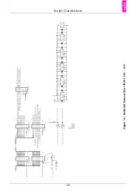
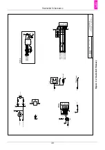
To connect 3.3V chips to the memory bus or to maintain compatibility between various
products it is recommended to implement buffer chips on the memory bus externally, like
shown in Figure 5.1, “Buffered Memory Bus (PIOC) 1.8V - 3.3V”
To connect 5V chips the same schematics can be used with suitable buffer chips.

