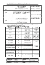
7&/0XOWLPHGLD7HFROGLQJ&57%85 '&HQWHU
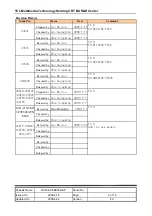
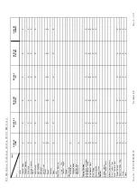
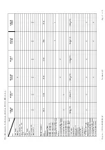
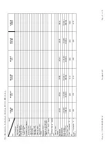
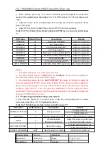
Model
Item
NX-56-AP2
21M62S
NX-56-AP
21M83
NX-56B-AP
21F1
NX-56-AP
29NE64S
NX-56-AP
14F1
NX-56-AP
21NCM86
-Out Headphone
Mini-Jack 3.5mm
Final Equipment
-Packing –Methods
2 Color Printing
Carton Color
-Documents and Manuals
Instruction Book
Screen Sticker
Plastic Bag
Warranty Card
Guarantee Doc.
Warning Label
Approbation Label
Others
-Languages DFU
-Indication on BACKOVER
Made-in in family sheet
FCC/Elect
Shock
Caution
Label
CE/Elect
Shock
Caution
Label
Warning Label
Others
Approbation
IEC65
IEC65
IEC65
IEC65
IEC65
IEC65
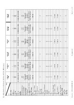
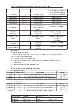
Miscellaneous
-Mains Voltage
110-240V
110-240V
110-240V
110-240V
110-240V
110-240V
-Mains Frequency
50/60Hz
50/60Hz
50/60Hz
50/60Hz
50/60Hz
50/60Hz
-Type Mains Cord
-Power
Consumption
TV
in
ON
65W
65W
70W
60W
65W
105W
-Power
Consumption
TV
in
Standby
<3W
<1W
<3W
<3W
<3W
<3W
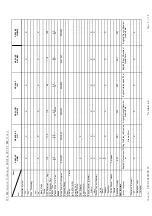
&KDVVLV1;$3 1;%$3
Version: 4.0
3DJHRI