background image

TCL Multimedia Technology Holding CRT BU R&D Center


Chassis Name 

NX56-AP&NX56B-AP

Serial No. 


Issued on 

2008-01-18 

Page  

Page 12 of 17 

Updated on 

2009-04-24 

Version 

4.0 

1. 

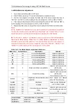
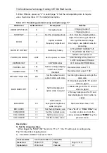
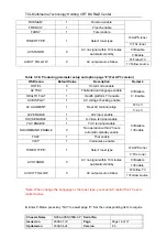
Enter P-Mode, press key “4” to select page “4”.Set the corresponding item to require 

value. See below table 3.7.1 for detailed description. 
 

Table 3.7.1: Producing parameter setup and option page “4”


OSD menu 

Default Value 

Description 

Remark 

0=Aging mode off 

WARM UP STATUS 

Set aging mode 

1=Aging mode on 

SHOP INIT 

Set the shopping status

0=>1= Set the shopping status   

DCXO 2 

Crystal oscillator 

frequency adjustment 

Adjust this value to get the max 

color synchronization range. 

Don’t adjust, use default value for 

producing 

0=”FACTORY HOTKEY” off 

FACTORY HOTKEY 

Set factory hotkey 

1=”FACTORY HOTKEY” on 

ON=On when power on   

STB=Standby when power on 

POWER ON MODE 

LAST 

Set the power on mode

LAST=Last power off status 

EEPROM INIT 

EEPROM initial   

0=>1=Active EEPROM initial 

POWER LOW 

101 

Recommended value= “16”   

POWER HIGH 

176 

Set the “Voltage display” 

“LOW” and “HIGH” 

threshold 

Recommended value= “168”   

DEFAULT SND. SYS 

DK 

Set the default sound 

system when auto store

Set the right value according to the 

sales area 

0= Blue background for TV and AV 

while no signal 

1=Black background for TV and AV 

while no signal 

BLUE BACK OPT 

Set the Background 

option while no signal 

2=Snowy background for TV and 

black background for AV while no 

signal 

BLACK BRI 

40 

Set the black 

background brightness 

while no signal 

Recommended value= “20”   

BRI CURVE 

>> 

Set the brightness curve

CON CURVE 

>> 

Set the contrast curve 

COL CURVE 

>> 

Set the colour curve 

VOL CURVE 

>> 

Set the volume curve 

Press

 “

►◄

” 

or

 “VOL+ VOL-” 

key 

to enter a sub-menu to do the 

setup, and press 

“MENU”

 key the 

previous menu 


Description: 

1). Set the shopping status 

    When trigger the “SHOP INIT” item form “0” to “1”, the TV will be put on selling status. 
The TV status after shopping status: 
A.  “FACTORY HOTKEY” had set to “OFF”.   

Summary of Contents for 14F7-NX56CLA

Page 1: ...C 73 14F7 Tempory Lacking...

Page 2: ...of uninsulated voltage within the products enclosure that may be of sufficient magnitude to constitute a risk of electric shock to the person The exclamation point within an equilateral triangle is i...

Page 3: ...nnel 8 Do not subject your television set to impact of any kind Be particularly careful not to damage the picture tube surface 9 Unplug this television set from the wall outlet before cleaning Do not...

Page 4: ...porting structure grounding of the lead in wire to an antenna discharge unit size of grounding conductors location of antenna discharge unit connection to grounding electrode and requirements for the...

Page 5: ...21 If you are unable to restorenormal operation by following the detailedprocedurein your operating instructions do not attempt any further adjustment Unplug the set and call your dealer or service te...

Page 6: ...TCL Thomson Electronics R D Center Shen Zhen Lab Chassis Name Serial No Issued On Page Updated On Version Product Functional Specification NX56 LA 2008 5 19 1 of 7 1 0...

Page 7: ...be reproduced or copied or used as the basis for the manufacture or sale of apparatus or devices without the written permission of TCL Thomson Electronics Version Information Version states by two Ar...

Page 8: ...Checked by Released by Prepared by lipeng 2008 5 19 Checked by Released by Revised by Checked by Released by Revised by Checked by Released by Chassis Name Issued On Updated On 3 of 7 29185 V1 0 03 B1...

Page 9: ...ide Screen Switching Comb filter Picture Enhancement LTI CTI Black Stretch Dynamic Skin Others Picture Control General Brightness X X Sharpness X X Contrast X X Tint X X Color X X Picture Control Spec...

Page 10: ...lish Portugal Espanol English Portugal Espanol Features General AT Biological Clock Calendar Clock Channel Swap X X Channel Naming Child Lock X X Favorite Channel X X Game Hotel Mode X X High Sensitiv...

Page 11: ...BS Component In YPbPr Cinch for 50Hz In Y C Cinch CVBS Stereo 1 1 1 2 In Y C Cinch CVBS Mono In Cinch CVBS Stereo In Cinch CVBS Mono Out Cinch CVBS Stereo Out Cinch CVBS Mono 1 follow TV 1 follow TV Y...

Page 12: ...Indication on BACKOVER Made in in family sheet FCC Elect Shock Caution Label CE Elect Shock Caution Label Warning Label Others Miscellaneous Mains Voltage 100 240V 100 240V Mains Frequency 50 60Hz 50...

Page 13: ...D Center Chassis Name NX56 AP NX56B AP Serial No Issued on 2008 01 18 Page Page 1 of 17 Updated on 2009 04 24 Version 4 0 NX56 AP NX56B AP Chassis Alignment Procedure Disclosure Proprietary Informatio...

Page 14: ...Thomson Electronics and shall not be reproduced or copied or used as the basis for the manufacture or sale of apparatus or devices without the written permission of TCL Thomson Electronics Version Inf...

Page 15: ...ccord with 21 tube 2 Updated the description accord with the software changing Prepared by Luo MJ 2008 07 04 Checked by Guo Guangyuan 2008 07 04 All NX56 AP chassis Released by Zhou Songming 2008 07 0...

Page 16: ...Note 1 This will be active only when the FACTORY HOTKEY had set to ON 1 2 When the power on with FACTORY HOTKEY had set to ON 1 the set will enter the P Mode automatically 1 2 Exit the P Mode Press th...

Page 17: ...geometry page 3 White Balance Adjustment White Balance page 4 Setup and option page 4 5 Setup and option page 5 6 Setup and option page 6 7 Setup and option page 7 8 Setup and option page 8 FAV Setup...

Page 18: ...rties checking for chassis RF AGC adjustment Parameter setup White balance Adjustment Aging Adjustment of focus voltage Adjustment of screen voltaget PAL geometry adjustment NTSC geometry adjustment S...

Page 19: ...ltage range 110VAC 240VAC 50Hz 3 Connect a voltmeter to B Cathode of D808 for NX56 chassis or cathode of D833 for NX56B chassis and switch on the set 4 Input Philips test pattern signal and standard m...

Page 20: ...h 60dB V amplitude B Enter P Mode press 6 key on RC to select AGCT C Adjust the AGCT value until the hint display AGC just change between 0 and 1 3 3 Screen Focus adjustment Note Alignment below shoul...

Page 21: ...offset setup When the TV white balance adjustment is done connect a black and white pattern to YUV input terminal Use the color analyzer to measure the black side of the screen Adjust the value of th...

Page 22: ...elow table 3 6 1 For NTSC signal the 50 will be replaced with 60 3 Adjust the value of the corresponding item to make the vertical geometry of the pattern look good 4 Apply NTSC signal to adjust these...

Page 23: ...tal geometry adjustment OSD menu OSD menu Default Value Description Remark HCEN 50 32 Horizontal shift HSH Adjust to right value HSIZE 50 32 EW width EWW Adjust to right value HPARA 50 32 EW parabola...

Page 24: ...mode LAST Last power off status EEPROM INIT 0 EEPROM initial 0 1 Active EEPROM initial POWER LOW 101 Recommended value 16 POWER HIGH 176 Set the Voltage display LOW and HIGH threshold Recommended valu...

Page 25: ...r Contrast 0 Use default value C Colour curve OSD menu Default Value Description Remark COL0 0 Set the minimal colour when user Colour 0 Set to 3 COL50 32 Set the colour when user Color 50 COL100 63 S...

Page 26: ...72 Recommended value 72 WarmGC 71 Warm temperature R and G cut off offset Recommended value 71 WarmRD 65 Recommended value 65 WarmGD 64 Warm color temperature R and G drive offset Recommended value 64...

Page 27: ...use default OSVE 0 Black current measuring lines in over scan for vertical zoom setting 1 Don t adjust use default CL 8 Set the cathode drive level Adjust to right value accord with the tube Recommend...

Page 28: ...d dual language enable HEALTH FLAT 1 Health platform TV enable AC DISPLAY 1 AC voltage checking enable 0 Disable 1 Enable 0 3 x 3 AV ALIGMENT 1 Rear AV terminal align 1 4 x 3 AV2 ENABLE 1 AV2 input en...

Page 29: ...0 Black area to switch off the black stretch 3 8 0 1 1 1 1 5 1 RPA 1 Ratio of pre and after shoot 2 2 1 0 1 1 1 1 1 3 3 1 1 7 RPO 1 Ratio of positive and negative peaks 4 1 0 7 0 0 1 5 2 10 SOC 2 Sof...

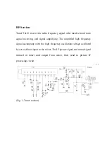
Page 30: ...nd signal amplifying The amplified high frequency signal accompany with the high frequency oscillation voltage oscillated by set oscillator input to the mixer The IF picture signal and sound signal fo...

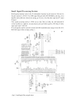
Page 31: ...processing get the color video broadcast signal and 2nd sound IF signal Video signal processing section is CVBS across video filter and delay line and horizontal vertical synchronous separation circu...

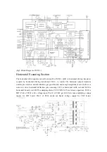
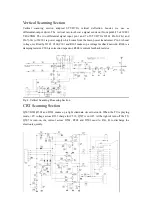
Page 32: ...ng in switch on and off situation get good linearly and enough amplitude of saw tooth wave current to drive horizontal deflection yoke scanning L456 is horizontal width coil and L458 is horizontal lin...

Page 33: ...r transformer Pin 6 is boost voltage rectified by D301 C309 C301 and R305 makes up a voltage feedback network R306 is a damping resistor C306 is correction capacitor R308 is current feedback resistor...

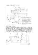
Page 34: ...LF801A and CX802 makes up a differential mode rejection LF802 and CY801 CY802 makes up a common mode rejection network D801 D804 is rectifying network 300Vdc voltage supply pin3 of T801 also through...

Page 35: ......

Page 36: ......

Page 37: ......

Page 38: ......

Page 39: ......

Page 40: ......

Page 41: ......

Page 42: ...ot contain an East West and Scan Velocity Modulation SVM output This concept is intended for 90 picture tubes Mono 110 concept The functional content of this concept is comparable with that of the AV...

Page 43: ...pplication it is necessary that an external bandpass filter is inserted Audio switch circuit with 2 stereo inputs 1 stereo input can also be switched into two mono sound inputs and a stereo output whi...

Page 44: ...tion with two control loops and alignment free horizontal oscillator Vertical count down circuit Vertical driver optimized for DC coupled vertical output stages Horizontal and vertical geometry proces...

Page 45: ...ing 8 bit A D converter with 4 multiplexed inputs 4 PWM 6 bits outputs for analogue control functions 2 3 Data Capture Teletext and Closed Caption devices Text memory for 1 page Inventory of transmitt...

Page 46: ...f coloration Programmable Cursor Special Graphics Characters with two planes allowing four colors per character 2 4 2 Features of the Teletext and Closed Caption devices Four character sets Up to 576...

Page 47: ...A IPAudio supply current 8 0 V AV 110 90 and mono 110 version 10 mA Ptot total power dissipation 1 1 W Input voltages ViVIFrms video IF amplifier sensitivity RMS value 75 150 V ViSSIF rms sound IF amp...

Page 48: ...AL GEOMETRY EAST WEST AGCOUT VIFIN C2 C3 C4 CVBS4 Y4 H OUT PEAKING SCAN VELOCITY RGB YP R P B CON BRI RO GO BO BLKIN RGB CONTROL OSD TEXT INSERT WHITE P ADJ CONTR BRIGHTN RGB MATRIX H V REF Y DELAY AD...

Page 49: ...OUT VIFIN H OUT RGB YP R P B CON BRI RO GO BO BLKIN VGUARD RGB CONTROL OSD TEXT INSERT CCC BLACK ADJ WHITE P ADJ CONTR BRIGHTN RGB MATRIX H V REF Y DELAY ADJ SATURATION CVBS2 Y2 YSYNC IFVO SVO SOUND P...

Page 50: ...output AVL capacitor AVL 16 16 AVL capacitor DECBG 17 17 17 bandgap decoupling SECPLL 18 18 18 SECAM PLL decoupling GND1 19 19 19 ground 1 for TV processor PH1LF 20 20 20 phase 1 filter PH2LF 21 21 2...

Page 51: ...GO 45 Green output RO PROUT 46 46 Red output PR output RO 46 Red output BLKIN VGUARD SVM 1 6 47 black current input vertical guard scan velocity modulation output BLKIN VGUARD 1 6 47 47 black current...

Page 52: ...onitor applications This device supplied with up to 35 V provides up to 2 5 App output current to drive the vertical deflection yoke The internal flyback generator delivers flyback voltages up to 75 V...

Page 53: ...e of either VS 2 or 40 volts 2 Thermal Data Symbol Parameter Value Unit Voltage VS Supply Voltage pin 2 Note 1 and Note 2 40 V V5 V6 Flyback Peak Voltage Note 2 70 V V3 Voltage at Pin 3 Note 2 Note 3...

Page 54: ...put I1 Input Bias Current V1 1 V V7 2 2 V 0 6 1 5 A 1 I7 Input Bias Current V1 2 2 V V7 1 V 0 6 1 5 A VIR Operating Input Voltage Range 0 VS 2 V VI0 Offset Voltage 2 mV DVI0 dt Offset Drift versus Tem...

Page 55: ...2 and I6 Figure 2 Measurement of V5H Figure 3 Measurement of V3L and V5L 1V a 39kW 5 1 b I1 a I2 and I6 measurement b I1 measurement S Vs 2 6 I2 I6 4 7 2 2V STV8172A 5 6kW I5 5 1V 7 2 2V 1 4 Vs 2 6 V5...

Page 56: ...OFF the positive supply alone In this state where both inputs are the same voltage as pin 2 or higher the output will sink negligible current from the deviation coil 4 1 1 Application Hints For calcul...

Page 57: ...tion of any ripple caused by a voltage drop in the ground see Figure 5 if you manage to apply the same fraction of ripple voltage to both booster inputs For that purpose arrange an intermediate point...

Page 58: ...of the yoke 4 2 1 Application Hints Gain is defined as in the previous case Choose R1 then either R2 or R3 For good output centering V7 must fulfill the following equation or Figure 6 AC coupled Appl...

Page 59: ...is the common mode current at peak of signal i icm ip and i icm ip therefore the peak differential signal is ip ip 2 ip and the peak peak differential signal 4ip The application is described in Figure...

Page 60: ......

Page 61: ......

Page 62: ......

Page 63: ...ce Q801 Is D801 D804 OK Yes Check IC801 and the peripheral components Replace D809 D812 No No Figure 1 Fuse Blown No raster abnormal B Is the B resistance to earth ok Check the load of B No Yes Check...

Page 64: ...upply of IC601 Yes Is the waveform at P57 P58 of IC201 ok Yes Replace IC601 Check Replace Q602 Q600 No Figure 4 No Sound No raster B Voltage OK Is the voltage of Pin8 IC202 5v Is the resistance to ear...

Page 65: ...to IC201 form AV input No Check IC201 Check AV Signal input Yes AV has Picture TV hasn t Picture Check tuner TU100 Check tuner working is ok Figure 6 No Picture Is both 14V and 14V ok Yes No Is the si...

Page 66: ...R216 T8 1466SAH MA1 18 CB0152 JNX RES C F 1 5K OHM 1 6W 5 R311 T8 1466SAH MA1 18 CB0221 JNX RES C F 220 OHM 1 6W 5 R604 R603 T8 1466SAH MA1 18 CB0222 JNX RES C F 2 2K OHM 1 6W 5 R301 R304 R407 R616 R...

Page 67: ...R229J2 0EX COIL PL 2 2 UH 5 L205 T8 1466SAH MA1 40 0NX56B MAF1XG TV PCB MA BD R Y T8 1466SAH MA1 41 WJ0050 B00 TCL41 WJ0050 B00 WIRE BARE JUMPER 5MM R L206 JP601 JP604 JP202 JP101 T8 1466SAH MA1 41 W...

Page 68: ...MHZ TO 92 2SC Q001 T8 14F1SAH KE1 18 CB0100 JNX RES C F 10 OHM 1 6W 5 R001 T8 14F1SAH KE1 18 CB0102 JNX RES C F 1K OHM 1 6W 5 R002 R011 T8 14F1SAH KE1 18 CB0103 JNX RES C F 10K OHM 1 6W 5 R003 T8 14F1...

Page 69: ...220 JSX RMOF 22OHM 5 2W R Y R891A T8 14F1SAH PW3 18 FG0330 JSX RMOF 33OHM 5 2W R Y R823A T8 14F1SAH PW3 18 FG0470 JSX RESISTOR RMOF 47OHM 5 2W 47OHM 5 R875A T8 14F1SAH PW3 18 FG0569 JSX RMOF 5 6OHM 5...

Page 70: ...1 KRX CAP CER 560PF 2KV 10 C815 T8 14F1SAH PW3 26 APL222 ME4 CAP CER 2200PF 400VAC 20 E C829 T8 14F1SAH PW3 27 AQQ104 KVX CAP M PP 0 1 UF 275VAC 10 C801 T8 14F1SAH PW3 36 LIF001 XX0 TCL36 LIF001 XX0 L...

Page 71: ...0 R T8 14F7AH RC2 63 B40150 AB4G SCREW ST 4MM 15MM ISO 62 R Y MTG FBT T8 14F7AH RC2 63 B40200 AB3G SCREW ST 4MM 20MM JIS B 1122 12 R Y MTG FRONT REAR CAB T8 14F7AH RC2 63 F30100 BT3G SCREW ST 3MM 10MM...

Page 72: ...DIODE BAV21 SW D512 D522 D532 T8 1NX56B CR1K 11 0BF423 0BX TRANSISTOR BF423 PNP 126 Q513 Q523 Q533 T8 1NX56B CR1K 11 SC2482 0BX TRANSISTOR 2SC2482 Q511 Q521 Q531 T8 1NX56B CR1K 18 CB0271 JNX RES C F...

Reviews: