background image

OPERATION OF YOUR SET

18.

This television set should be operated only from the type of power source indicated on the marking label.   

If you are not

sure of the type of power supply at your home, consult your television dealer or local power company.  For television
sets designed to operate from battery power, refer to the operating instructions.

19.

If the television set does not operate normally by following the operating instructions, unplug this television set from the
wall outlet and refer servicing to qualified service personnel.  Adjust only those controls that are covered in the operating
instructions as improper adjustment of other controls may result in damage and will often require extensive work by a
qualified technician to restore the television set to normal operation.

20.

When going on a holiday :  If your television set is to remain unused for a period of time, for instance, when you go on
a holiday, turn the television set 

and unplug the television set from the wall outlet.

IF THE SET DOES NOT OPERATE PROPERLY

21. If you are unable to restore normal operation by following the detailed procedure in your operating instructions,

do not attempt any further adjustment.  Unplug the set and call your dealer or service technician.

22. Whenever the television set is damaged or fails, or a distinct change in performance indicates a need for

service, unplug the set and have it checked by a professional service technician.

23. It is normal for some TV sets to make occasional snapping or popping sounds, particularly when being

turned on or off.  If the snapping or popping is continuous or frequent, unplug the set and consult your
dealer or service technician.

FOR SERVICE AND MODIFICATION

24. Do not use attachments not recommended by the television set manufacturer as they may cause hazards.

25. When replacement parts are required, be sure the service technician has used replacement parts specified

by the manufacturer that have the same characteristics as the original part.  Unauthorized substitutions
may result in fire, electric shock, or other hazards.

26. Upon completion of any service or repairs to the television  set, ask the service  technician  to  perform

routine safety checks to determine that the television is in safe operating condition.

5

off 

Summary of Contents for 21M62S

Page 1: ...SERVICE MANUAL MODEL 21M62S CHASSIS M123SP...

Page 2: ...of uninsulated voltage within the products enclosure that may be of sufficient magnitude to constitute a risk of electric shock to the person The exclamation point within an equilateral triangle is i...

Page 3: ...nnel 8 Do not subject your television set to impact of any kind Be particularly careful not to damage the picture tube surface 9 Unplug this television set from the wall outlet before cleaning Do not...

Page 4: ...porting structure grounding of the lead in wire to an antenna discharge unit size of grounding conductors location of antenna discharge unit connection to grounding electrode and requirements for the...

Page 5: ...21 If you are unable to restorenormal operation by following the detailedprocedurein your operating instructions do not attempt any further adjustment Unplug the set and call your dealer or service te...

Page 6: ...n Others Blue mute Picture Control General Brightness X Sharpness X Contrast X Tint X Color X Picture Control Special Smart Pictures modes 4 VM Color Temperature X Others Picture Noise Reduction Pictu...

Page 7: ...gical clock Calendar X Clock X Channel Skip Channel Swap Channel Adjustment 1 Channel Naming Channel Lock Child Lock X Favorite Channel X Game X Hotel Mode High Sensitive Notebook X On Off Timer X Pan...

Page 8: ...Cinch CVBS Mono In Y C Cinch CVBS Mono In Cinch CVBS Stereo In Cinch CVBS Stereo X In Cinch CVBS Mono In Cinch CVBS Mono Out Cinch CVBS Stereo Out Cinch CVBS Stereo X Out Cinch CVBS Mono Out Cinch CVB...

Page 9: ...English Indication on BACKOVER Made in in family sheet X FCC Elect Shock Caution Label FCC Elect CE Elect Shock Caution Label CE Elect Warning Label Others Approbation FCC FCC FDA FDA UL CUL UL CUL CB...

Page 10: ...NTRAST SUB TINT AND SUB COLOR FOR NSTC AND PAL SIGNAL 4 2 WHITE BALANCE ADJUSTMENT NORMAL 8 5 ADJUSTMENT OF SUB BRIGHTNESS 8 6 PICTURE GEOMETRIC ADJUSTMENT 8 7 X RAYS OVER VOLTAGE PROTECTING CIRCUIT T...

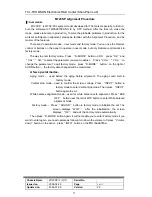
Page 11: ...arameter you want to adjust Press VOL VOL to change the parameters To quit factory mode press D MODE button on the right of SURR button the factory data changed will be memorized A few special modes A...

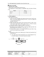
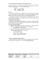
Page 12: ...Apply 8 scale gray signal 80dB and then adjust AGC data in D mode until the synchronization signal distortion appear exactly Test Pin 1 of TU101 IF output and record the voltage value as V2P P Illustr...

Page 13: ...2 0V P P as shown below 4 Select COLC to adjust the color by tuning the amplitude of a and d to the same 5 Select TNTCV T to adjust the tint by tuning the amplitude of b and c to the same 6 Apply the...

Page 14: ...C BD C for cool temperature into memory 5 Adjustment of Sub brightness Apply the Grey scale Color bar NTSC signal to the AV input in normal status Enter factory alignment menu 8 Select BRTS to adjust...

Page 15: ...r it is disqualification 9 PS power test Random test Instruments Power meter Input signal pattern Color bar Sound 1KHZ 100 modulation Input signal intensity 60dBuv 1 Mv rms Test points find the graphi...

Page 16: ...to the 2 ends of CRT glowers test the heater voltage of highest CR and Brightness It should meet 6 3 0 3Vrms 12 CCD and VOL CHIP function test VOL CHIP and CCD function test please find the service ma...

Page 17: ...T3 SV3 SV4 SVD ASSH SHPX SHPN M123SP 1B 1B 1B 1B 07 1A 1A 20E10 1B 1B 1B 1B 07 1A 1A FAC 07 Data Model MOD1 MOD2 MOD3 OPT OPTM1 OPTM2 HDCNT HSTOP M123SP 60 F3 88 37 C2 83 09 FF 20E10 60 F1 88 37 C2 83...

Page 18: ...2 Data Model SVM SVM1 OSD2 OSDF2 PYNX PYNN PYXS PYNS M123SP 10 10 20 64 28 18 22 10 20E10 10 10 20 64 28 18 22 10 FAC 13 Data Model CLTM CLVO CLVS ABL DCBS FLG0 FLG1 M123SP 04 03 03 27 14 82 0C 20E10...

Page 19: ...AI GATE VOL OUT AV GAIN OPTM3 M123SP 03 2A 75 2D 40 20E10 03 2A 75 2D 40 FAC 25 Data Model G2_FLAG00 G2_FLAG01 G2_FLAG02 G2_FLAG03 G2_FLAG04 G2_FLAG05 M123SP 30 06 00 02 40 00 20E10 30 06 00 02 40 00...

Page 20: ......

Page 21: ...ains 8 bit CPU ROM RAM I O ports timer counters A D converters an on screen display controller remote control interfaces IIC bus interfaces and the Closed Caption decoder The TV signal processor conta...

Page 22: ...lumns 12 lines Composition 16 18 dots Size of character 3 line by line Color of character 8 character by character Display position H 256 V 512 steps BOX function Fringing smoothing Italic underline f...

Page 23: ...t SIF out Sync out H L out AU Monitor out ALC filter A Vcc 8V YC Vcc 5V AU out 2 P20 Int5 Stop P40 PWM14bit Reset P50 PWM7bit TC2 Int0 TV AGND 6dB PIF Proc PAL NTSC demod Auto VCO alignment Vert Proc...

Page 24: ...om MCU are controllable through the IIC bus of the internal connections 2 Power Supply TMPA8873 has some power supplies and GND pins Power supplies related MCU must be applied at the first Power suppl...

Page 25: ...4 I O Input Input Key on wake up input A D converter analog input 2 9 4 1k 5k Key on Wake up 22pF Disable Initial Hi Z 3 P53 KWU0 AIN0 TC1 INT2 SCK1 I O Input Input Input Input I O Key on wake up inpu...

Page 26: ...9 up DVdd Power Supply Vdd Supply 5V 9 CPU core Digtal curcuit Slicer 10 up VVss Power Supply GND for Slicer circuit 54 up AGND Power Supply GND for Oscillator circuit 55 up AVdd Power Supply Vdd for...

Page 27: ...59 P50 PWM8 TC2 INT0 I O Output Input Input 7 bit D A conversion PWM output Timer Counter input External interrupt input 59 9 4 1k Disable Initial Hi Z 60 P40 PWM0 I O Output 14 12 bit D A conversion...

Page 28: ...03 29 28 Pin No Pin Name I O Function Interface Circuit 63 P30 INT3 RXIN I O Input Input External interrupt input Remote control signal preprocessor input 63 9 4 1k Disable Initial Hi Z 64 P63 LED2 I...

Page 29: ...FC 1 Terminal to be connected capacitor for H AFC filter This terminal voltage controls H VCO frequency 100 300 14 17 11 33k 15 V saw Terminal to be connected capacitor to generate V saw signal V saw...

Page 30: ...22 Ext Au1 Input terminal for Audio signal 1 17 22 18 35k 35k 5k 200 23 C in Input terminal for Chroma signal 23 47 18 1 5k 40k 24 V2 in Input terminal for Video signal 24 47 18 11k 1 5k 1 5k 25 ALC f...

Page 31: ...for 1bit DAC or detected SIF signal 36 40 31 32 Ext Au2 in Input terminal for Audio signal 1 17 32 18 35k 35k 5k 200 33 H correc SIF in Input terminal for H correction and 2nd SIF 33 36 40 500 70k 30...

Page 32: ...ND GND terminal for IF circuit 41 42 IF in Input terminals for IF signals Pin41 and Pin42 are both input poles of differential amplifier 50k 20pF 1 4k 50k 20pF 1 4k 41 42 36 40 43 RF AGC Output termin...

Page 33: ...s required because of its open collector output Pull up resister minimum 4 7kohm 11 17 48 100 5k 49 DVCC Vcc terminal for Digital block This terminal voltage is clipped about 3 3V by regulator circuit...

Page 34: ...p Filter A sound trap filter is integrated on the chip for multi frequency SIF systems The sound trap filter characteristics are changed by WRITE BUS register setting It is better that the setting dat...

Page 35: ...ection The 1 H delay line is integrated on the chip for PAL chroma demodulation The 1 H delay line can acts as a chroma comb filter on NTSC chroma system 10 Base Band Color System TMPA8873 features a...

Page 36: ...each other at the same time is recommended 14 Control the Signal Processor The signal processor is connected with the micro controller by means of internal wiring All functions of the signal processo...

Page 37: ...6 PCB Layout...

Page 38: ......

Page 39: ...104 FAST RECTIFIER D404 T8 0021GPS MA1 10 0FR104 FBX DIODE FR104 FAST RECTIFIER D401 T8 0021GPS MA1 10 0FR104 FBX DIODE FR104 FAST RECTIFIER D402 T8 0021GPS MA1 10 0FR104 FBX DIODE FR104 FAST RECTIFIE...

Page 40: ...K OHM 1 4W 5 R311 T8 0021GPS MA1 18 CD0820 JNX RES C F 82 OHM 1 4W 5 R298 T8 0021GPS MA1 18 CE0682 JNX RES C F 6 8K OHM 1 2W 5 R410 T8 0021GPS MA1 18 DB0223 FNX TCL18 DB0223 FNX RES M F 22K OHM 1 6W R...

Page 41: ...20 C304 T8 0021GPS MA1 25 BHB100 M1X CAP ELEC 10 UF 100V 20 C406 T8 0021GPS MA1 25 BHB100 M1X CAP ELEC 10 UF 100V 20 C420 T8 0021GPS MA1 25 MFB228 K1X CAP ELEC 0 22UF 50V 10 C205 T8 0021GPS MA1 25 MF...

Page 42: ...13 T8 0021GPS MA1 41 WJ0075 B00 WIREBAREJUMPER7 5MM J012 T8 0021GPS MA1 41 WJ0085 B00 WIREBAREJUMPER8 5MM JP403 T8 0021GPS MA1 41 WJ0100 B00 WIREBAREJUMPER10MM JP912 T8 0021GPS MA1 41 WJ0100 B00 WIREB...

Page 43: ...PER15MM JP402 T8 0021GPS MA1 41 WJ0150 B00 WIREBAREJUMPER15MM L402 T8 0021GPS MA1 41 WJ0150 B00 WIREBAREJUMPER15MM J922 T8 0021GPS MA1 41 WJ0150 B00 WIREBAREJUMPER15MM J908 T8 0021GPS MA1 41 WJ0150 B0...

Page 44: ...M1X CAP ELEC 1 UF 50V 20 C847 T8 0021GPS PWN 26 AIC221 KBX CAP CER 220 PF 500V 10 B C830 T8 0021GPS PWN 26 AIC221 KBX CAP CER 220 PF 500V 10 B C841 T8 0021GPS PWN 35 LB1005 0IX FERR BEAD H75 3 5X1X5...

Page 45: ...6GP KE1 41 WJ0075 B00 WIREBAREJUMPER7 5MM J1001 T8 21123GP DPN 10 1N4148 ABX DIODE 1N4148 SWITCHING D1101 T8 21123GP DPN 10 1N4148 ABX DIODE 1N4148 SWITCHING D1110 T8 21123GP DPN 10 1N4148 ABX DIODE 1...

Page 46: ...MM R J1101 T8 21123GP DPN 41 WJ0050 B00 TCL41 WJ0050 B00 WIRE BARE JUMPER 5MM R J1105 T8 21123GP DPN 41 WJ0050 B00 TCL41 WJ0050 B00 WIRE BARE JUMPER 5MM R J1104 T8 21123GP DPN 41 WJ0050 B00 TCL41 WJ00...

Page 47: ...JUMPER7 5MM J509 T8 DE10SGP CRY 41 WJ0075 B00 WIREBAREJUMPER7 5MM J505 T8 DE10SGP CRY 41 WJ0075 B00 WIREBAREJUMPER7 5MM J502 T8 DM62SGP OT2 18 CB0473 JNX RES C F 47K OHM 1 6W 5 R930 T8 DM62SGP OT2 41...

Page 48: ...SSIN T8 0DM62GP FC1 63 B40150 AB4G SCREW ST 4MM 15MM ISO 62 R Y MTG CHASSIS F CAB T8 0DM62GP FC1 63 S30100 AB4G S T SCREW S 3 X 10 AB MTG SPK F CAB T8 0DM62GP FC1 63 W30100 AB4G S T SCREW W 3 X 10 AB...

Page 49: ...13 STV817 2AS IC DEFLECT STV8172A VERTICAL DEFLECTION IC301 T8 0021GPS MA1 18 EE0109 JS2 RES FUS 1 OHM 1 2W 5 R418 T8 0021GPS MA1 18 EF0339 JGX RES FUS 3 3 OHM 1W 5 R421 T8 0021GPS MA1 18 EF0478 JGX...

Page 50: ...P402 T8 0021GPS MA1 46 39039H 02XG HS 2P 2468 26 130MM TJC3 2Y SAN 2Y P403 T8 0021GPS MA1 64 B30080 304G TRIANGLE M C SCREW B 3 X 8 FOR Q402 T8 0021GPS MA1 64 B30080 304G TRIANGLE M C SCREW B 3 X 8 F...

Page 51: ...TJC2 2A P803 T8 0021GPS PWN 50 03150D 1GS1G TCL50 03150D 1GS1G FUSE 3 15AT 250VAC 5 F801 T8 0021GPS PWN 57 10654X 00F TWIST TIE NY66 T8 0021GPS PWN 63 B30100 AB4G SCREW ST 3MM 10MM JIS B 1122 53 0 0...

Page 52: ...A1 19 AB0000 JTX RES SMD 0 OHM 1 10W 5 0603 J906 T8 0021GPS MA1 19 AB0100 JTX RES SMD 10 OHM 1 10W 5 R005 T8 0021GPS MA1 19 AB0100 JTX RES SMD 10 OHM 1 10W 5 R001 T8 0021GPS MA1 19 AB0100 JTX RES SMD...

Page 53: ...S MA1 19 AB0332 JTX SMD RES 3 3K OHM 1 10W 0603 R209 T8 0021GPS MA1 19 AB0333 JTX RES SMD 33K OHM 1 10W 0603 R205 T8 0021GPS MA1 19 AB0393 FTX SMD RES 39K OHM 1 10W 1 R842 T8 0021GPS MA1 19 AB0470 JTX...

Page 54: ...0021GPS MA1 28 AB0222 KBX CAP SMD 2200PF 50V 10 0603 C213 T8 0021GPS MA1 28 AB0222 KBX CAP SMD 2200PF 50V 10 0603 C407 T8 0021GPS MA1 28 AB0222 KBX CAP SMD 2200PF 50V 10 0603 C014 T8 0021GPS MA1 28 A...

Page 55: ...01 UF 50V 10 0603 C425 T8 0021GPS PWN 28 AB0104 KBX SMD CAP 50VDC 0 1UF 10 06 C837 T8 0021GPS PWN 28 AB0104 KBX SMD CAP 50VDC 0 1UF 10 06 C814 T8 0021GPS PWN 28 AB0221 JCX CAP SMD 220PF 50V C 0603 5...

Page 56: ...0 M1X CAP ELEC 4 7UF 50V 20 NP C1109 T8 21123GP DPN 27 AHQ563 JSX CAP M PP 0 056 UF 400V 5 C1115 T8 21123GP DPN 36 WID301 XX2 COIL WIDTH 300 UH L1101 T8 21123GP DPN 36 WID361 XX1 COIL WIDTH 360 UH LC...

Reviews: